With the conventional AM broadcast stations being gradually phased out, it becomes reasonable to have a low power AM transmitter at home or in an antiques shop to be able to play music of your choice through old vintage collectable AM radios. There are probably millions ways to make such a transmitter, but why not convert a surplus vintage medium wave radio into a transmitter? This way the unit will not only operate as a transmitter, but also present itself as a vintage display item.
It turns out that such conversion is not only possible, but is rather simple, as will be demonstrated further. Since the chassis, cabinet, dial glass, tuning mechanism, power transformer and lots of electronics from the old "donor" radio can be utilized in the transmitter, the project also becomes inexpensive.
A generalized schematic diagram of a medium wave transmitter which covers a standard broadcast band 530...1700kHz, converted from a 4 or 5-valve superheterodyne radio, is shown in Fig. 1.

Fig. 1. Generalized schematic diagram of an AM transmitter converted from a vintage tube radio.
Mains power transformer and the rectifier are retained, a frequency changer is converted to an oscillator, output audio stage is utilized as output RF amplifier. A tuning dual-gang capacitor, tuning mechanism, volume control and even a ferrite rod antenna and one IF transformer are reused too. Operation of the circuit is explained in more detail below.
Oscillator
The oscillator employs a negative resistance topology, which does not require "tickler" windings, taps or capacitive dividers to provide positive feedback for oscillation. Of the four topologies shown in Fig. 2 (dynatron, transitron, phantastron and cascode), "transitron" and "cascode" are the most common and are recommended.

Fig. 2. Negative resistance oscillator topologies.
Transitron and cascode provide the best amplitude and frequency stability, besides, the former one utilizes a frequency changer tube from a "donor" radio. It requires a dual-control pentode (with fine suppressor grid) or a hexode / heptode. In brief, its principle of operation is as follows. Because of the cathode self-bias resistor R1, the third grid is biased negatively with respect to cathode, and about half of the electron flow is reflected back to screen grid 2. Suppose, because of some fluctuation, voltage on the LC tank (grid 3) becomes a little negative. That would result in more electrons reflected back to grid 2, and grid 2 current increases. This increase in grid 2 current obviously causes grid 2 voltage to go down. Through the coupling capacitor C10 this negative voltage trend on grid 2 pushes grid 3 also more negative, thus positive feedback is created. Conversely, with positive voltage excursions on grid 3 more electrons pass to the anode, grid 2 current reducing and pulling the LC tank voltage up.
Transitron can utilize a dual control tubes: pentodes (6DT6, 6AS6), triode-hexodes (6AN7, ECHxx, 6K8), heptodes (6BE6, 6SA7, ECH81, 6CS6), etc. If a pentagrid or triode-hexode is used, an unused oscillator anode may be grounded as sown in Fig. 3A.
![]()
Fig. 3A. Transitron oscillator utilizing a triode-hexode.
Low current, low transconduction heptode of 6J8G does not work well in the transitron connection. However, by applying supply voltage to the triode plate, and taking into account that grid 2 of the heptode works as anode of the other triode, very strong oscillation can be obtained even with moderate (60...70V) DC supply voltage. In such configuration (Fig. 3B), due to the common cathode, cascode and transitron action is combined. Needless to say, any other triode-hexode can work in the transitron/cascode mode with excellent results, provided the tube is shielded.

Fig. 3B. Combination of cathode-coupled cascode and transitron
The oscillator also can be fully transistorised, using common collector - common base (cascode) configuration, which will be addressed later.
For the best frequency stability, any RF injection into the circuit shall be minimized. Before attempting to convert a radio into the transmitter, it is important to make sure that the tuning capacitor has a shielding partition between the stator plates sections. Otherwise with the vanes out (at minimum capacitance) the stator sections will be directly facing each other and an undesirable coupling between the modulator output and the oscillator tank will take place. If 6AN7 or ECH81 tube is to be used in the oscillator, it must be shielded, otherwise the internal shielding of the tube, connected to its cathode will work as antenna, providing a noise injection path into the oscillator. A shield can be easily cut and rolled from a food can tin metal, as shown in an example of Fleetwood radio conversion (Fig. 3C). An additional valve 6BL8 in this example is used for asymmetrical modulation, but for brevity this topic will not be discussed, as in reality the asymmetrical modulation in reality gives only insignifical advantage.

Fig. 3C. Home made shield for 6AN7 oscillator tube (converted Fleetwood radio).
Alternatively, R10 can be shunted by 0.1uF capacitor, but it decreases internal impedance of the tube and reduces Q of the tank, which is not recommended. The shielding is not needed for the tubes having the plate as an outer electrode, which naturally provides RF shielding of the internal electrode system.
Cathode resistor R10 depends on the tube used. For sharp cut-off in respect of grid 1 tubes (6DT6, 6BE6, 6SA7, 6A8, etc.), this resistor is typically smaller, for remote cut-off tubes (6AN7, ECH81, 6J8G, etc.) it is larger. It is recommended, at the alignment stage, to temporarily connect a variable resistor in there, and obtain the maximum oscillator voltage on the LC tank (recommended 12...15Vrms). Then fit a fixed resistor of about the optimum value. To set the optimum oscillation level (12...15V) it is recommended to control supply voltage Vosc by selecting R6 (Fig. 1). Tube 6AS6 requires minimum Vosc of 160...170V to produce high output. 6BE6 requires the highest supply voltage Vosc = 210...230V. 6AN7 is somewhere in between.
The most important is to run the oscillator at half of the output frequency (about 265...850kHz) and then double the frequency down the track. In this way, frequency stability is far superior as the oscillator is not subject to the frequency "pull" and synchronization effects by radiated emissions, which would cause parasitic frequency modulation.
Depending on the size of the tuning capacitor C12 (360...500pF in different radios), the value of the oscillator inductor L2 should be around 740...1000uH. The inductor shall be adjustable and have a reasonably high Q. An interesting, important and beneficial coincidence is that a typical inductance of a coil in a 455kHz IF transformer is also in the order of 800...1100uH. Therefore, in 90% of cases it is possible to utilize one coil of an IF transformer as the oscillator inductor L2. The IF transformer shall be modified as shown in Fig. 4.

Fig. 4. Modification of an original IF transformer (left) as an oscillator inductor (right).
Capacitors in the IF transformer can be removed or left in place (as usually they are overmolded). A coil adjusted from the top is more convenient to use as L2. Polarity of the coil is not critical, but it would be marginally better to use inner end (sitting on the coil former) as a "hot" end (connected to the oscillator circuit), and outer end -- grounded. The other (bottom) coil of the IF transformer shall be shorted out. When rewiring (shown in red) it is very important to, using an Ohm-meter and monitoring the resistance of the coil, make sure that all the strands of the Litz wire are soldered and none is broken, otherwise Q of the coil will drop.
In most cases IF coil inductance turns out a bit higher than required, and sometimes mechanical modifications to the IF transformer might be required to remove one of the slugs, increase slug travel out of the coil, etc. If complete removal of a ferrite slug is not sufficient to tune to a required frequency, it is recommended to unwind certain number of turns from the coil or insert a copper or aluminium tube, rod or screw into the coil, reducing its inductance. (The later reduces Q of the tank.) Alternatively, two coils of the IF transformer can be connected in parallel.
In rare cases an opposite situation happens when inductance of one coil is not large enough, for example in the case of the "slim" compact Philips IF transformers (Fig. 5).

Fig. 5. An example of Philips IF transformer which requires connecting both coils in series.
In this case the capacitors must be removed and the two coils connected in series.
Frequency doubler and modulator
Block diagram of the doubler/modulator submodule is shown in Fig. 6.

Fig. 6. Frequency doubler-modulator module block diagram.
Oscillator signal passes through a capacitive divider C4C5, providing low capacitive loading to the oscillator tank, through the buffer and through the frequency doubler, which is in effect a full-wave rectifier. A limiter turns half sine peaks into almost rectangular signal which then drives the modulator. The modulator is a differential emitter coupled switch. Due to full current steering between the transistors, its modulated output is directly proportional to the common emitter current flowing in through R4. Average carrier level is determined by the current flowing into "CRR" node through R3 (Fig. 1). R6 (Fig.6) is a built-in load resistor for AM output. Amplitude modulation is nothing other than modulation of current through R4. This is achieved, in turn, by supplying audio signal to "CRR" node via C7 from an audio amplifier. The audio amplifier is based on Sziklai pair which has high gain and low distortion. About 2...3V of audio is needed at "CRR" for the full 100% modulation. Optimum oscillator voltage at "OSC" input is 10...15Vrms.
The audio amplifier has a low impedance input junction "IN", and its overall signal gain, as in an inverting operation amplifier is determined by the ratio of the feedback resistor R10 (Fig. 6) over combined input resistance R11, R12, R13 (Fig. 1). Maximum gain is about R10/R12 = 21. (Input sensitivity -- about 100...150mV). Note an unusual (inverted) connection of the volume (modulation) control potentiometer R11 (Fig. 1). Advantage of such connection is lower hum, noise and distortion. In effect, the volume control changes not the input voltage to the audio stage, but the feedback depth. At low volume position the feedback is the deepest and the noise is minimal. In contrast, with conventional connection, at low volume the audio stage might be picking up chassis ground noise/hum between the module earthing point and R11 earthing point.
The doubler-modulator module is supplied from an internal shunt (Zener) 30V regulator. The buffer, doubler and limiter stages draw about 2.5mA, so a slightly larger 3..5mA current should be sourced into "30V" pin via R2 (Fig. 1) from the "B+" rail of the radio. As mentioner, R3 (Fig. 1) determines the carrier level. Current at "CRR" is typically 1.5mA. For undistorted modulation, quiescent current of the audio stage shall be about two times larger. Thus it is recommended to have R4 (Fig. 1) approximately half of R3 (Fig.1).
The doubler-modulator submodule is implemented on a small 35mm x 23mm PCB (Fig. 6A).
 |
 |
Fig. 6A. Doubler-modulator submodule PCB.
It is small and lightweight and can be mounted by soldering to some supports rather than held by screws (Fig. 6B).

Fig. 6B. Doubler-modulator module installed. R2, R3, R4, R6, C4 (Fig. 1) can be seen on its left. Oscillator tank is above, with the oscillator tube 6AN7 socket and R1, R10, C10, C3 at the top of the picture.
The module is robust and wiring layout is not critical, and can be quite messy, only "OSC" and "OUT" circuits should be kept separated as much as possible for frequency stability.
Transistorised oscillator
If space is at premium, or a user is not keen on making a shield for the oscillator tube, a transistorised "appendix" can be added to effectively emulate cascode (common collector - common base) operation, as shown in Fig. 7.

Fig. 7. Solid-state (add-on) oscillator
This add-on circuit is enclosed in pink rectangle. Signal can be taken from the buffer stage (Q1 emitter on the main PCB), and with additional buffering by a pnp (BC857) transistor and level shifting by the 22K resistors, fed through a 1000pF capacitor into another pnp transistor (BC857) operating in common base configuration. Thus a cascode configuration with positive feedback is created. The later transistor provides soft clipping, and the oscillator amplitude at L2C12 tank is always maintained at an optimum level of 20V (14Veff).
The add-on module is connected to the three existing pads of the main PCB, and also requires an additional wire (shown in red in in the schematic Fig. 7 and blue in the actual assembly) from Q1 emitter to "Q1E" pad on the add-on PCB. The pictures below (Fig. 8) illustrate the connection.
 |
 |
Fig. 8. Connection of the add-on transistorised oscillator to the main module PCB.
Due to extra 0.8mA current drawn by the add-on circuit, supply ballast resistor (R2 in Fig. 1) shall be about 25% smaller.
Output stage
RF modulated output (carrier level) of about 5V (depending on the output tube) is developed on the tuned LC tank L1C9. An existing antenna RF coil of the radio or its ferrite rod antenna or a loop antenna can be used, as it is already designed to cover the standard broadcast frequency range. Antenna coupling coils which are usually wound on the same coil former, should be physically removed. It is also recommended to ground L1 (Fig. 1) not to the chassis of the radio, but to the frame of the tuning capacitor, thus avoiding RF currents circulating through the common grounding lead (usually a braid) of the tuning dual-gang capacitor. As emphasized above, this measure helps reduce cross-coupling between the modulator output and the oscillator tank -- for better frequency stability. RF voltage level is determined by "CRR" current, as well as by the built-in load resistor R6 in the module (Fig. 6). This resistor also affects the Q-factor of L1C9 tank, and the Q in turn affects the RF bandwidth, and hence the audio modulation bandwidth. With R6 = 15K, at the low end of the band Q = 20 (approximately), and the modulator will have about 12kHz audio bandwidth at -3dB level. At the top end of the band Q-factor drops significantly to about 6, and modulation audio bandwidth increases to about 25kHz, including the effect of finite audio stage bandwidth. Note that even 12kHz is quite excessive to listen on a typical vintage radio barely able of reproducing up to 6kHz. Only a top-of-the-line receiver with variable IF bandwidth ("local/distant" reception switch) or a radio with a synchronous detector is capable of matching the full modulation bandwidth of this transmitter.
Output power stage V2 is a wideband linear amplifier. Tube V2 is virtually a voltage-to-current converter, and the RF current is fed into the antenna. Almost any output pentode or beam tetrode can be used. Plate current of 30mA is recommended. If high supply voltage (250...300V) is available from the rectifier, then audio output tubes, like 6V6GT, 6AQ5, 6M5 (EL41, EL80), 6BQ5 (EL84), 6GW8 (ECL86), etc. are recommended. If the supply voltage is lower (200...230V, in small radios), then TV frame tubes 6BM8 (ECL82), 6GV8 (ECL85), EL82 are preferred. 6V6GT/6AQ5 is good for either situation. A grid stopper resistor R8 (Fig. 1) is a must, particularly for high-transconductance tubes as 6M5, 6GV8, etc. (Grid stopper can be fitted to screen grid too.) Cathode self-bias resistor R5 (Fig. 1) is not bypassed by a capacitor or partly bypassed -- for linearity and lower equivalent capacitive loading of the L1C9 tank. Recommended net transconductance, taking into account cathode degeneration, should be about 1.5...2.5mA/V. To adapt virtually any output tube the following "tricks" illustrated by Fig. 8A and Fig. 8B may be used (apart of "playing" with screen grid voltage):

Fig. 8A, B. Transconductance degeneration (left); partial self-bias resistor bypass (right).
For high-transconductance tubes which naturally would require low self-bias resistor, in order to degenerate gain, partial self-bias voltage feed to the grid can be used (Fig. 8A). Value of R15 is selected on test to reach about 30mA of plate current. For the frame output TV tubes which usually have quite low internal "mu", and R5 is getting too high, it can be partially bypassed by R15C15 (Fig. 8B). In some cases it might be possible to use the same filter RC circuit R6C4 or R14C5 to supply both the screen grid and the oscillator.
Another transconductance degeneration method is presented in Fig. 8C.

Fig. 8C. Transconductance degeneration by splitting cathode impedance.
R5 provides required self bias, while at RF both R5+R15 combined provide local negative current feedback, linearising the amplifier. If located conveniently, a second unused IF transformer coil (disconnected from its capacitor!) can be used as L3. Advantage of Fig. 8C over Fig. 8A is that DC resistance from the tube control grid to ground is low, thus "gassy", "leaky", "dirty" old tubes with considerable grid current and inter-electrode leakage still can be successfully utilised in this application.
Antenna terminal of the transmitter is decoupled by two high voltage capacitors C7, C8 in series for extra safety in an extremely unlikely event of one of them breaking down. R9, value of which is not critical, bleeds static charge after power-up / power-down -- for safety.
Note that 2K2 plate load resistor (R7 in Fig. 1) drops about 60...70V DC. If the available supply voltage is below 200V, plate voltage on the tube V2 will be too small, leaving little or no headroom for the modulated AM signal. In this case a DC supply through a 1...2mH RF choke (parallel feed or "parafeed") shall be preferred. A second IF transformer of the donor radio may be converted into such choke. Both coils should be connected, electrically and magnetically, in series -- that is end of the first coil to the start of the second one. Inner turns (on the former) of the bottom coil is better to connect to the tube plate, and the outer turns of the top coil -- to the supply voltage (Fig. 8D). Exact inductance and position of the slugs is not critical. Such topology provides even higher output that the original (Fig. 1), as the resistive load R9 is now larger: 3K3 instead of 2K2.
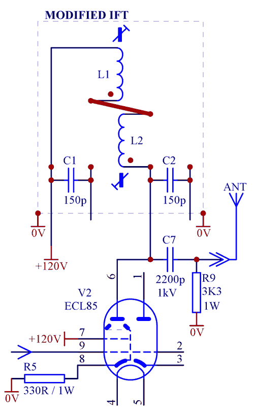
Fig. 8D. Parafeed connection of the power stage.
RF modulated voltage on the control grid of V2 shall be optimized too. On one hand, it shall be high enough to produce reasonably powerful output. On the other hand, it shall be small enough to minimize distortion and harmonics emission by the output tube V2. The best is to check the envelope of the modulated signal on the antenna output. Examples are shown below in Fig. 9.
 |
 |
Fig. 9. Modulated envelope: almost perfect (left); slightly asymmetrical (right).
Envelope on the left may be considered perfect, yet negative excursions of the envelope are always more elongated than the positive ones. It is due to the fact that volt-current characteristic of the tube is not linear -- positive grid voltage excursions cause larger plate current changes and hence larger negative plate voltage excursions. In effect, the tube generates some amount of the second harmonic of the carrier frequency. It is not of a great concern as the emission level is small and unlikely to cause any interference to other receivers nearby. On the right hand side screenshot, this asymmetry is more pronounced and the positive lobes look more "squashed", compressed and rounded. The tube seems to be driven rather close to cutoff. Nevertheless, even this example can be considered acceptable, but the situation may be improved by reducing cathode self-bias resistor R5 (Fig. 1) for the tube and slightly reducing "CRR" carrier level by increasing R3 (Fig. 1). This observable asymmetry does not directly translate into modulation distortion. Modulation distortion caused by the tube nonlinearity is far smaller than the envelope asymmetry, because, as far as the fundamental frequency is concerned, compression of the positive peaks is compensated by elongation of the negative ones, making the fundamental frequency component ideal in amplitude.
As can be seen in the photos, undistorted modulation depth is 100%. Note that AM detector of a typical AM radio can only handle of about 70% of modulation before diagonal clipping takes place. Thus the transmitter can be considered a perfect "reference" signal source for an AM radio.
Power supply
Mains power transformer and a rectifier of the donor radio are retained. A reservoir capacitor C5 (Fig. 1) should be as large as possible without overstressing the rectifier tube. If a choke is found in the donor radio, it is a bonus -- a higher supply voltage and less ripple is expected. Silicon diodes 1N4007 can also be used. In this case they should be shunted by 0.01...0.022uF / 250Vac capacitors to avoid possible modulation hum. For the same purpose, shunting capacitors C1, C2 across active, neutral and neutral-to-earth are required. They make all the three cores of the power cord equipotential on RF thus minimising possible modulation by switching rectifier diodes in numerous household appliances and electronic devices. RF filtering/decoupling of the supply rails by C3, C6 and C14 (Fig. 1) is recommended. Transformerless donor radios (some European and the American "AA5") with live chassis are not suitable because of electrical safety hazard.
Alignment
With the help of the trimmer capacitors C11, C13 and slugs of L1 and L2 it is possible to perfectly align the transmitter to the graduations of its dial. However it is not necessary, and a simpler procedure can be used. From experience, winding capacitance of an IF coil used as L2 is quite large, therefore, in most cases, C11 may be omitted. On the other hand, quite often coil L1 of a donor radio is firmly glued to the ferrite rod and impossible to move. Therefore it is recommended first to adjust L2 for maximum output at the low end of the band, and then adjust C13 for maximum output at the top end of the band.
Antenna
A wire several meters long, stretched above or next to the area where the receiver is located works well. Such antenna has almost capacitive impedance, and voltage on it is 5...20V depending on its length and frequency. It is safe to touch. Earthing of the transmitter is not essential -- household electrical wiring working as a counterpoise. Transmission range is about 10 meters, which is large enough to cover a household and yet small enough to create interference. Alternatively an antenna can be a large wire loop connected between "ANT" and "EARTH". Such antenna radiates magnetic field and more suitable for serving transistor radios with ferrite rod antennas. It is recommended first to find a free spot on the dial of a receiver and then tune the transmitter into that frequency.
An example of a converted into a transmitter radio is shown below (Fig. 10).

Fig. 10. Rear view of a radio converted into the transmitter.
The oscillator valve is shielded, the speaker is retained only to avoid see-through effect. A socket in the middle is the audio input. A black wire on the right side is the antenna lead, terminated by an alligator clip (not visible).
In conclusion, note that the schematic shown in Fig. 1 is presented as an example, and does not have to be strictly followed. Any simple, not rare, low collectors value radio can be sacrificed, "butchered" and easily converted into such a transmitter -- with many components retained and reused. Old electrolytic capacitors should be replaced.
Selecting a radio for conversion into a transmitter
Most of the radios can be converted, with some exceptions. "Permatune" radios with inductive tuning are not suitable. Some low cost models, as Westinghouse or AWA, where the screen (partition) between the stators of the tuning gang is absent, are not suitable too. In the AM modulator, parasitic coupling between the oscillator and doubler LC tank can cause spurious FM.
Some simple radios have tuning gangs with dissimilar sections -- full capacitance for the antenna LC tank, and lower capacitance for the local oscillator. (Such trick was employed to save a few cents on the padder capacitor.) Those can be converted by adding an "anti-padder" in series with the antenna section to equalise tuning law of both sections. Exact value of the "anti-padder" can be determined empirically. For a Kriesler, model 11-99 (refer to the schematic at the end of the article) it is about 250...257pF. However, full effective capacitance will be about a half and will require to double the inductance of the oscillator and the doubler (grid) LC tank. The former can be done by connecting both coils of a donor IF transformer in series, the later -- by adding a fixed inductor in series with antenna coil or loopstick.
Even then, it will be difficult, if not impossible to get coverage of the full MW band, as the inductances are now doubled, but wiring and interelectrode capacitances remain the same. Also, tuning will not follow the original frequency graduations on the dial. Therefore, conversion of the radios with dissimilar sections of the tuning gang is not recommended and can be considerd as a "last resort".
Gallery -- photos of AM modulator modules installed in various Australian made radios
You can see that the AM modulator module can be conveniently fitted to almost any table radio chassis.

Fig. 11A. AM modulator fitted to AWA model 467MA radio. Two triodes 6AV6 form a cascode oscillator. Oscillator -- 6BE6, transitron. Output -- 6BM8.

Fig. 11B. AM modulator fitted to AWA model 573MA radio. Two triodes 6AV6 form a cascode oscillator. Output -- 6AQ5.

Fig. 11C. AM modulator fitted to BGE Dapper radio. This circuit uses cascode oscillator with 6BD7 and 6AV6 triodes. The former has an internal grounded screen, which is very helpful. Output -- 6BM8.

Fig. 11D. AM modulator fitted to the same BGE Dapper radio, however the output tube is located in the top left corner -- where the frequency converter tube was in the original radio. Output -- 6M5 tube with inductive transconductance degeneration as per Fig. 8C.

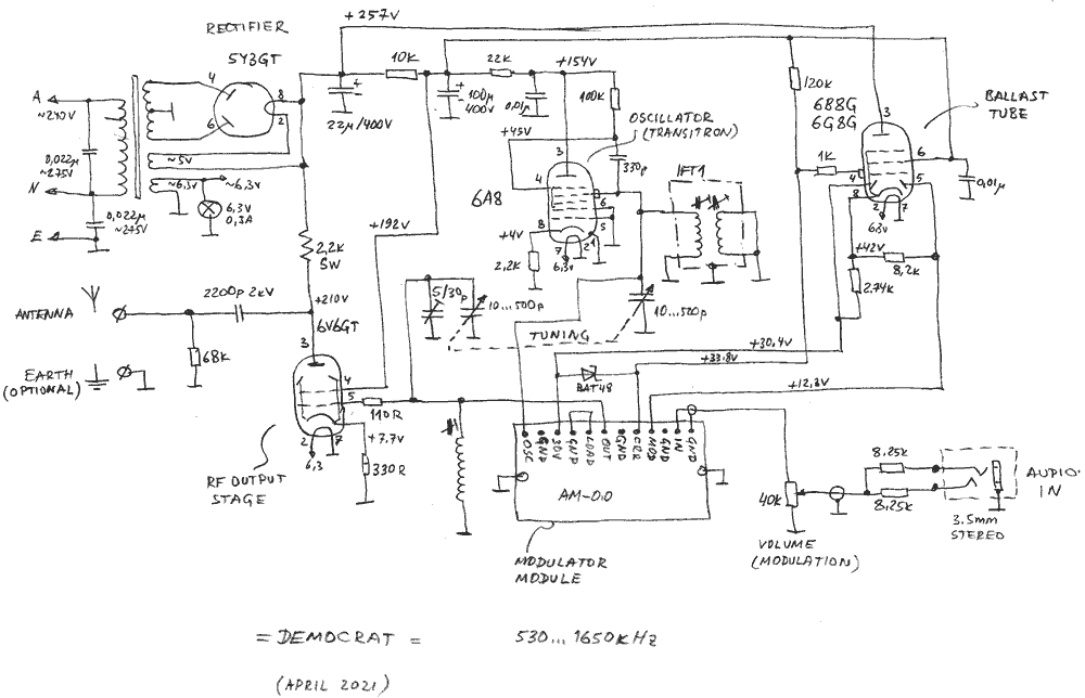
Fig. 11E. AM modulator fitted to Democrat radio. 6A8G is a transitron oscillator, 6F6G -- output.

Fig. 11F. AM modulator fitted to Stromberg-Carlson radio. Oscillator -- transitron 6A8G, output -- 6AQ5 (in place of the original 6V6GT).

Fig. 11G. AM modulator into Hot Point (AGE) radio. Oscillator -- 6A8G transitron, output -- 6V6GT, an additional tube 6G8G is assisting with asymmetrical modulation.

Fig. 11H. HMV "Super-5" radio has the most convenient chassis to convert to an AM modulator. Oscillator -- 6AN7A transitron, Output -- 6M5 with gain degeneration as per Fig. 8C.

Fig. 11I. AM modulator fitted to Airzone radio. Oscillator -- 6J8G transitron/cascode as per Fig. 3B, with LC tank from a different radio, output -- 6V6GT.

Fig. 11J. AM modulator fitted to Fleetwood radio. Oscillator -- 6AN7 transitron/cascode, 6BL8 for asymmetrical modulation, output -- 6M5 with transconductance degeneration.

Fig. 11K. AM modulator fitted into Healing "Golden Voice" model 505E radio (vertical chassis). Oscillator -- 2 x 6AV6 cascode, 6AU6 is for assisting asymmetrical modulation, output -- 6BV7 with transconductance degeneration.

Fig. 11L. AM modulator in (former Tasma) Mariposa radio. Oscillator -- 6AN7 transitron/cascode, output -- 6BM8 with automatic carrier level adjustment. As there is no room under the chassis, the modulator is mounted on top side.

Fig. 11M. AM modulator in a Democrat radio. Transitron oscillator -- 6A8 (metal for shielding); output -- 6V6GT; ballast tube regulating supply voltages to the modulator module -- 6B8G; rectifier -- 5Y3G.

Fig. 11N. AM modulator in His Master's voice, model 65-54 radio. Oscillator -- 6AN7 (transitron/cascode), output -- 6BM8, voltage regulator -- 6BA6, rectifier -- 6X4. Audio output transformer primary is used as a power supply filter choke.

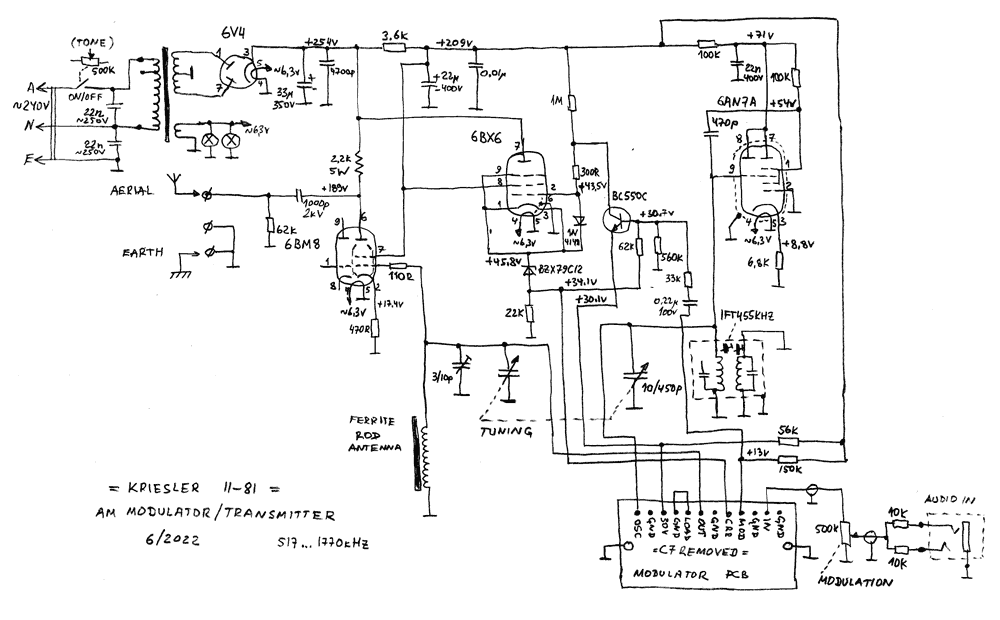
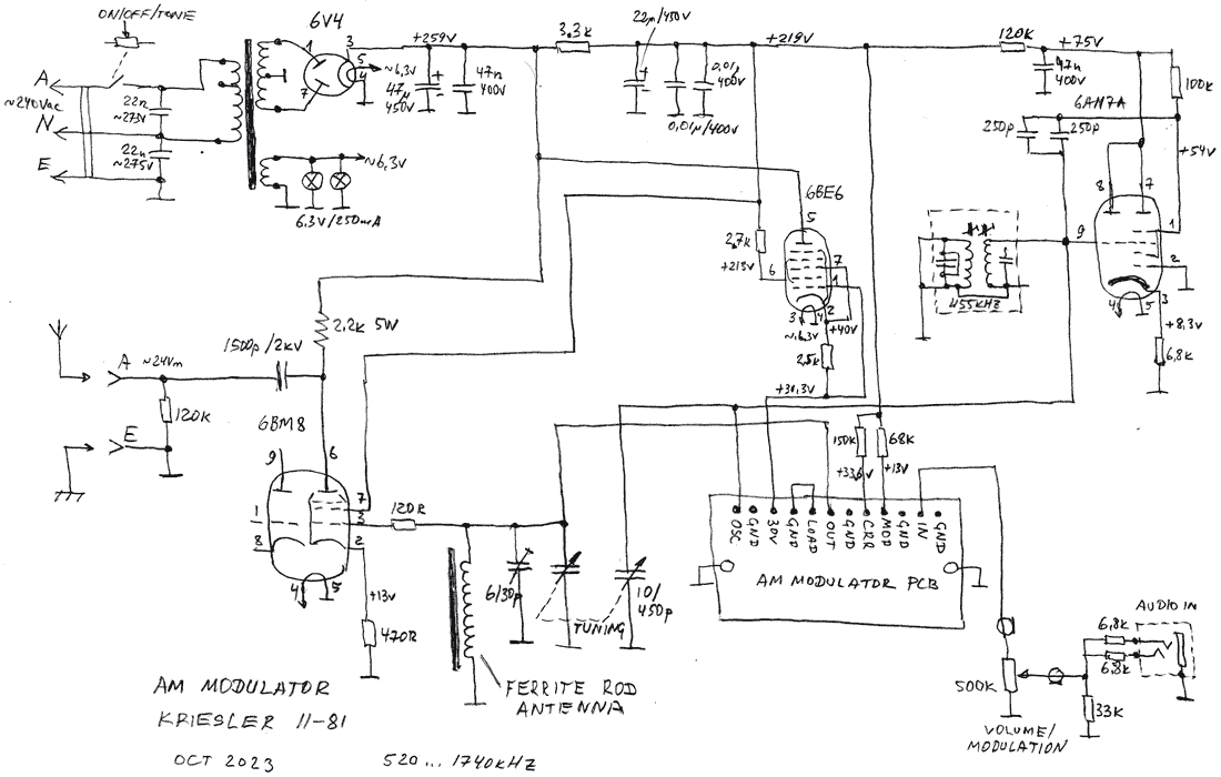
Fig. 11P. AM modulator in Kriesler 11-81. Oscillator -- 6AN7A (transitron/cascode), output -- 6BM8, asymmetrical modulation inverting amplifier -- 6BX6, rectifier -- 6V4.

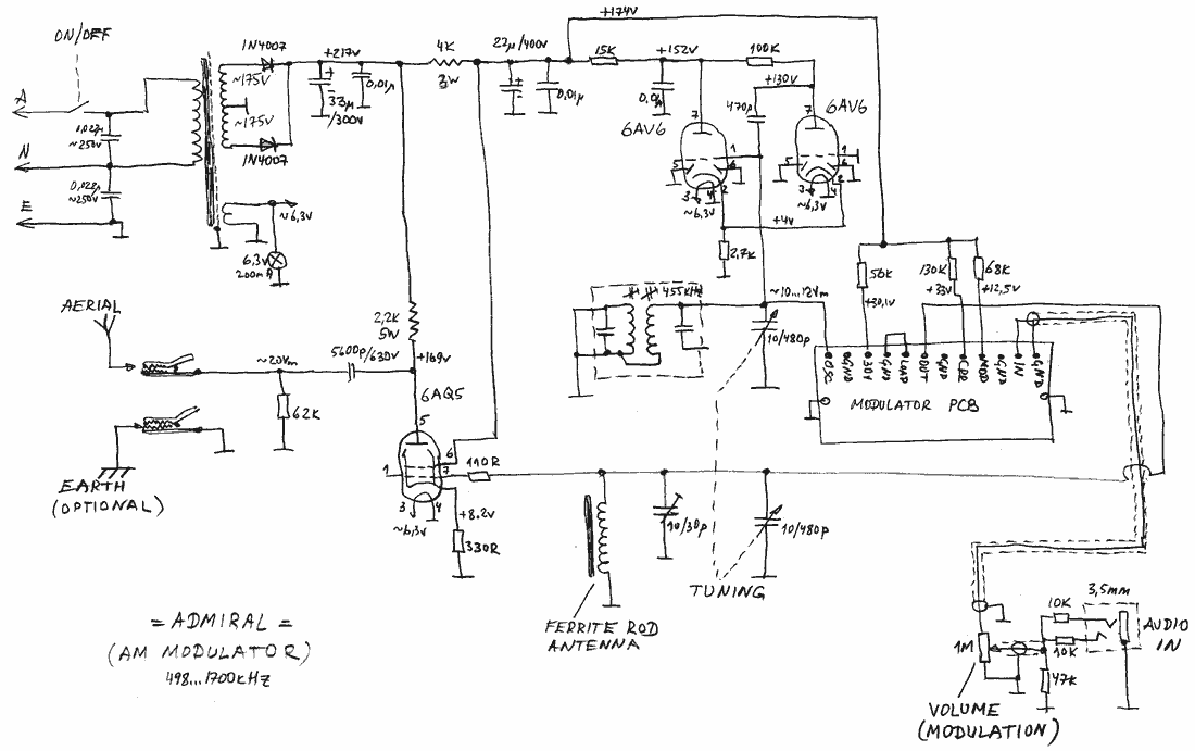
Fig. 11Q. AM modulator in Admiral radio, year 1965, uses PCB. Oscillator -- 2 x 6AV6, cascode, output -- 6AQ5, rectifier -- 2 x 1N4007 to reduce unnecessary heat dissipation.

Fig. 11R. AM modulator in Kriesler 11-81. Oscillator -- 6AN7A (transitron/cascode), output -- 6BM8, Current source (ballast) -- 6BE6, rectifier -- 6V4.

Fig. 11S. AM modulator in PYE Ranchero MR-2 radio. Oscillator -- 2 x 6BE6 (cascode, screen grids of the pentagrids are used as anodes, while anodes are grounded to work as the shields), output -- 6AQ5, rectifier -- 6V4.

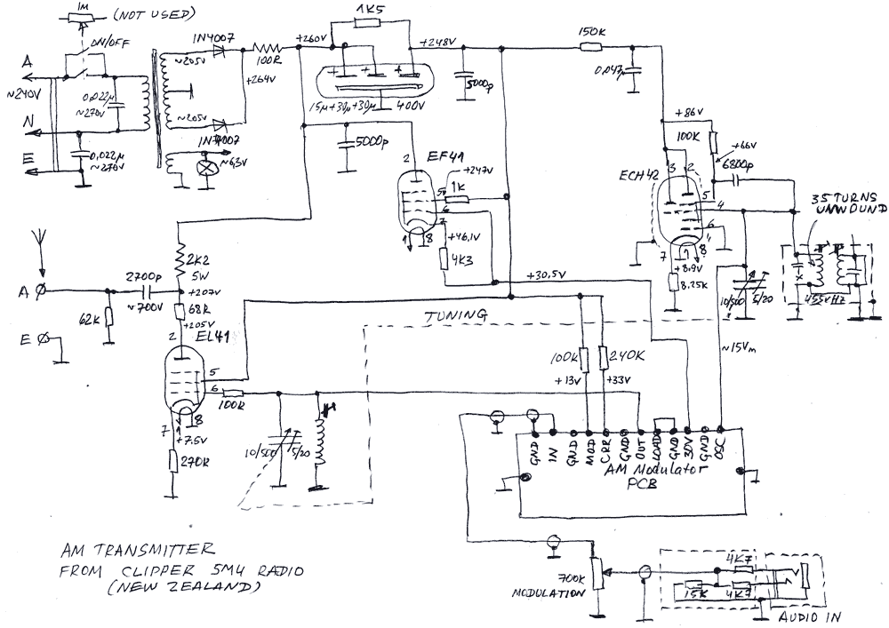
Fig. 11T. AM modulator in Clipper 5M4 radio (New Zealand). Oscillator -- ECH42 (transitron/cascode), output -- EL41, current source -- EF41, rectifier -- 2x1N4007. Original rectifier EZ40 is removed to eliminate that undesirable source of heat too close to the plastic cabinet front wall.

Fig. 11U. AM Modulator from Kriesler 11-99 radio, which has a tuning gang with dissimilar sections. Oscillator -- transistorised, output -- ECL85/6GV8, rectifier -- a silicon diode. The output tube plate is fed through a choke (the second IFT is used for that), and the output power is actually higher than in other transmitters with 2K2 load resistor.

Fig. 11V. AM Modulator from Kriesler 11-90 radio, which has a tuning gang with dissimilar sections. Oscillator -- transistorised (a small add-on PCB replaces a tube), output -- ECL85/6GV8, rectifier -- 6V4. The output tube plate is fed through a choke (the second IFT is used for that), and the output power is actually higher than in other transmitters with 2K2 load resistor.
Schematic diagrams of some Australian radios converted to transmitters
A sample circuit diagram of a "real working" transmitter built on the chassis of very common and abundant Kriesler "Panoramic" Australian radio, model 11-81, is presented below in Fig. 12. To obtain full resolution images of of this and other similar conversion projects, click on the links. You might be able to find a circuit for conversion of an unwanted radio you have or a similar one.

Fig. 12. AM transmitter from Kriesler 11-81 radio.
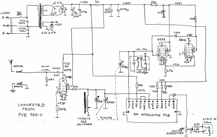
Practical schematic diagrams of the AM transmitters converted from other radios:
- Democrat
- Airzone
- Healing "Golden Voice" model 505E
- Thom and Smith/Tasma/Motorola "Mariposa"
- Democrat with ballast tube 6B8G
- Kriesler model 11-81 with inverting modulation amplifier
- Admiral
- Kriesler model 11-81 with ballast tube
For questions and to purchase a doubler/modulator module for such project feel free to use the contact page of this website.