Operation of a solid-state radiation dosimeter
Instead of a Geiger-Mueller tube, modern solid-state dosimeters usually employ a p-n junction (diode) as a radiation sensitive element (Fig. 1).

Fig. 1. Block diagram of a solid-state radiation dosimeter.
When a high energy particle or a photon strikes the depleted zone of the reverse biased diode, it knocks a number of electrons, depending on the energy of the ionizing particle. The electron-hole pairs do not recombine, but quickly drift to the terminals of the diode, thus creating a tiny burst (pulse) of electric current. This current is fed to the charge sensitive amplifier (CSA), which is in fact an integrator with a small (usually 0.5...1pF) integrating capacitor Cint. A small voltage step therefore appears at the CSA output. For example, if an ionizing particle with 100keV energy fully deposits its energy in the detector diode, and Cint=0.5pF, then the CSA voltage step is about 8.8mV. Obviously, the integrator requires occasional discharge (reset) or alternatively it is done by connecting a large resistor (50...1000MOhms) in parallel to Cint.
Voltage steps at the CSA output are not convenient to measure and process, and for that reason a shaper-amplifier follows the CSA. It combines differentiating action (R1C1), which picks up the step, with integrating action (R2C2) which filters noise. Usually R1C1 = R2C2. As a result, the shaper converts a voltage step in an exponential (ideally Bell-shaped) pulse, amplitude of which is proportional to the detected charge and hence the energy deposited in the detector.
A multi-channel analyser is basically an instrument which measures amplitude of each pulse and builds up a "histogram" -- how many pulses of certain amplitude have been detected. Analysis of this histogram (spectrum) with proper calibration allows to estimate energy spectrum of ionizing radiation in question and assess its dose rate.
Noise
If radiation dose rate (intensity) is small, then the "events" (detector hits) are infrequent, and it takes a long time to gather sufficient spectrum statistics from the MCA. To speed the measurements up it would be logical to increase the size (volume, surface area) of the diode detector or to connect multiple detectors in parallel. But that is where the problem arises -- a larger detector inevitably has a larger capacitance, which leads to higher noise.
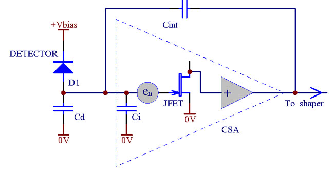
Fig.2. Charge sensitive amplifier noise equivalent circuit.
A charge sensitive amplifier (Fig. 2) usually employs a quality junction field-effect transistor (JFET) as a front end active device. Internal voltage noise of the JFET is represented by En. Noise gain -- ratio of output-to-input noise -- is ((Cd + Ci) / Cint + 1). To minimise noise, quality JFETs, e.g., 2SK932 or 2SK3666 are chosen for the highest transconductance and lowest input capacitance Ci.
Nevertheless, a larger detector or many detectors in parallel would have larger capacitance, which inevitably result in the noise increase. As a result a dosimeter will not be able to detect low energy radiation, pulses being swept by noise.
For example, if one connects ten identical detectors to the same CSA (Fig. 3, assuming Ci = Cd), total capacitance at input will rise from 2*Cd to 11*Cd, and noise floor will increase as much as 5.5 times.
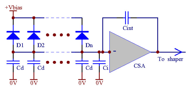
Fig.3. Multiple identical detector diodes connected to a CSA input.
A somewhat better results can be achieved by connecting multiple JFETs in parallel as well (Fig. 4).
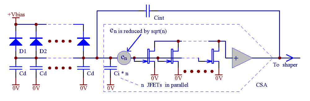
Fig. 4. Connecting JFETs in parallel reduces equivalent noise referred to input.
In this case, if ten (n = 10) identical detectors and ten identical JFETs are connected in parallel, total input capacitance would increase 10 times -- from 2*Cd (Fig. 2) to 20*Cd. However, equivalent noise En, being random and uncorrelated, would increase only SQRT(n) times. As a result, CSA output noise floor would increase about 3.1 times. It is still a significant degradation, though better than in Fig. 3. Needless to say, the result comes at the expense of a tenfold CSA current draw increase.
Similar results can be achieved if outputs of several full CSA-SHAPER channels are added together (Fig. 5).
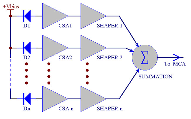
Fig. 5. Summation of the outputs of several shapers.
Obviously, since noise in the channels is uncorrelated, noise floor at the output of the adder increases SQRT(n) times. In the example of ten identical channels it would result in the similar 3.1 times noise floor and resolution of the dosimeter degradation. This arrangement is more complex, expensive and power hungry, but allows to use identical standard CSA and shaper modules.
Low-noise dosimeter solution
From the above examples it would seem that noise and consequential resolution degradation is an unavoidable penalty for using a large high-capacitance detector or multiple small detectors. But fortunately it is not so, and a solution to handle large detectors without noise degradation does exist (Fig. 6).

Fig. 6. Combining channel outputs through a maximum selector unit.
It differs from Fig. 5 by using a non-linear maximum selector unit instead of a linear adder. If an event occurs in any channel, and a pulse consequently rises above the noise floor, this pulse will be passed to the output (multi-channel analyser) through a respective "ideal diode". At the same time, noise from all the channels is not added together and is equal to the noise of one channel. Theoretically, unlimited number of channels can be combined this way, and there is neither limit, nor penalty for increasing effective area/volume of the detector.
In practice, number of the channels is limited by a pile-up condition, when coincidental events in different channels become more frequent. In case of coincidental pulses, by nature of maximum signal selector, only the largest pulse will pass to the MCA, and the smaller one will not be registered. Thus excessive number of channels in case of not so small dose rate may result in dosimertic accuracy degradation.
Implementation of an ideal diode or any other maximum selection technique, which is beyond the scope of the article, may be not trivial too, considering high-speed requirements. One of possible implementations of an ideal diode is presented in Fig.7.
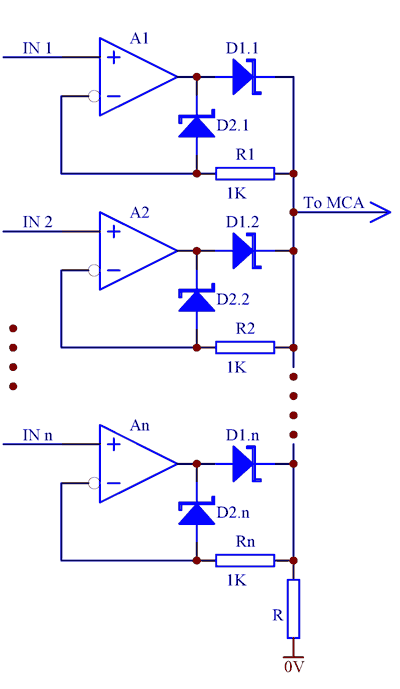
Fig. 7. Maximum selector using operational amplifier based "ideal diodes".
A dominant signal is precisely passed to load R by a respective operational amplifier via one of D1 diodes and drives the load. Diodes D2 in the recessive channels limit negative excursions of the op-amp outputs, which helps make the ideal diode relatively fast. Some additional forward bias (not shown in Fig. 7) may be applied to the diodes, keeping them closer to the conduction "kink". That will further reduce switching delay. Low capacitance Schottky diodes, like 1N5711 or BAS70 as well as high speed op-amps like AD8033 work satisfactorily in this circuit.
Conclusion
The method of combining several (n) channels through maximum selector gives at least SQRT(n) advantage in terms of noise over the common standard techniques. This method can also be applied "backwards" -- in order to improve resolution of a large capacitance detector, it can be "split" it into several smaller segments, with a separate CSA-SHAPER channel attached to it and the outputs combined via a maximum selector. Noise floor and resolution of the system will increase while the net effective area of the system can remain the same.