Audio burst generator
Overdriving tube audio amplifiers may cause certain undesirable effects. Interstage coupling capacitors might charge by grid currents, causing the output stage bias to slide to cut-off. In push-pull topologies, high current draw from the power supply can cause transients on the power supply rail. These effects may result in the amplifier being virtually muted or out of normal operation mode immediately after removal of the overdriving signal. It might take some time for the amplifier to recover. The "deeper" the negative feedback in an AC coupled amplifier, the less tolerant to overdrive it becomes, as even a small overdrive would produce an enormous error signal on the grid(s) of the output tube(s).
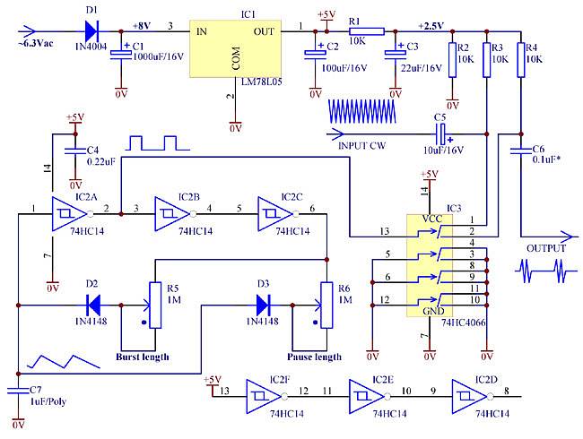
To test the recovery after overdrive performance of an amplifier, a burst audio oscillator is required. One way to implement such a device is to use a continuous wave audio generator, followed by a gate (switch), operated in ON/OFF mode at an infra low frequency cycle. A relatively simple and inexpensive solution is shown below.

The infra-low frequency gating signal oscillator uses a CMOS Schmitt trigger-inverter gate IC2 (74HC14). C7 is a timing capacitor. Charging and discharging times are controlled by R5 and R6 respectively, making possible to independently control the duration of the ON time (burst) and OFF time (pause).
The switch is a generic CMOS bi-directional CMOS switch IC3 (74HC4066), with only one switch of four used. (If lower ON resistance is required, they can be paralleled.) The switch is biased through R3 and R4 half way between the supply rails (to +2.5V) allowing to handle a signal of maximum 2.5...2.7V in amplitude. In most cases it is sufficient to give a decent overdrive to an amplifier under test.
If larger signal switching is required, then a dedicated analog switch IC should be used, such as DG442, DG445, etc. These require bipolar power supply and are more expensive, but there will be no need for DC biasing any more -- R1 - R4 and C3 will not be needed.
The ICs require 5V DC to operate. In the given example, this supply is obtained from a heater 6.3Vac through D1 rectifier and a 5V DC regulator LM78L05.
It is recommended to synchronize the gating oscillator with the input continuous wave test signal. Ideally, a burst shall begin at zero crossing of the carrier. To achieve that, a small portion of the input signal might be injected into C7, say through a small capacitor (1...10nF).
Also it is desirable that turning the switch OFF happens at a zero-crossing of the input signal, as well as equal number of positive and negative half-cycles are passed in each burst. This will ensure minimum DC "tail" and "clicks" in the output burst. It can be achieved by trimming of the burst length (R5) or of the input signal frequency.
It might be also useful to deliberately leak some input signal around the gating switch, by connecting say a large resistor across the input and the output. In this case after a burst a small signal will still be fed to the amplifier under test. Thus it will be possible to see if the amplifier under test is completely "muted" by the overdrive, and how long it takes to recover, or if the amplifier is still is "alive" right after the trailing edge of the overdrive.
This burst generator might also be used for assessing listening room acoustic reflections.
