Output stages using complementary transistors, bipolar junction (BJT) or MOSFETs, are quite common in audio amplifiers. These complementary stages usually come in either Darlington (Fig. 1) or Sziklai pair (Fig. 2) topology.
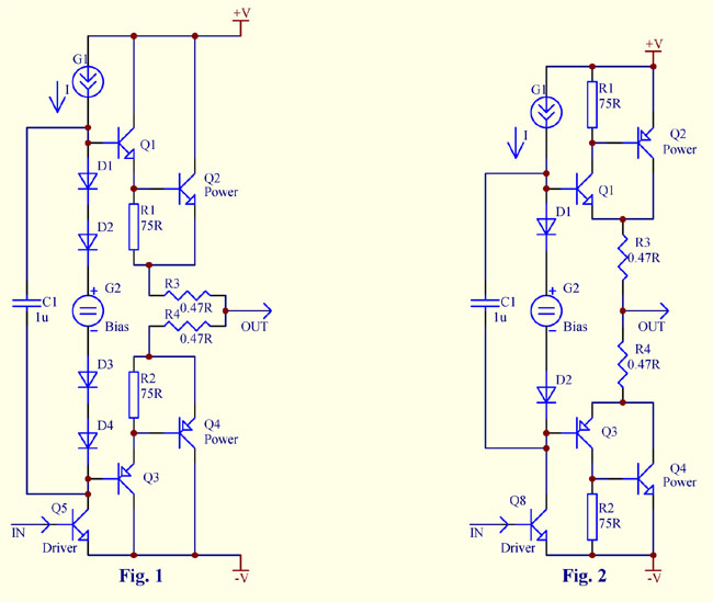
Differences between Darlington and Sziklai are discussed in detail in another article and will not be covered here. Suffices to say that the Sziklai (compound follower) configuration has more advantages and is generally recommended.
For low distortion, the two "legs" of a push-pull stage must have equal gain: equal current gain for BJTs or equal transconductance in case of MOSFETs. Though specially designed "complementary" power transistor pairs claim closely matched characteristics, in reality PNP and NPN counterparts or N and P-channel MOSFETs are not completely identical in performance. Usually PNP or P-channel parts are inferior to their NPN or N-channel siblings. The former have lower beta, transconductance, large capacitances, etc. This makes an output stage not quite symmetrical.
To improve the symmetry of a complementary push-pull output stage, a special "super complementary" topology can be used which has transistors of both polarities in both legs of the circuit. The diagram below illustrates the principle.
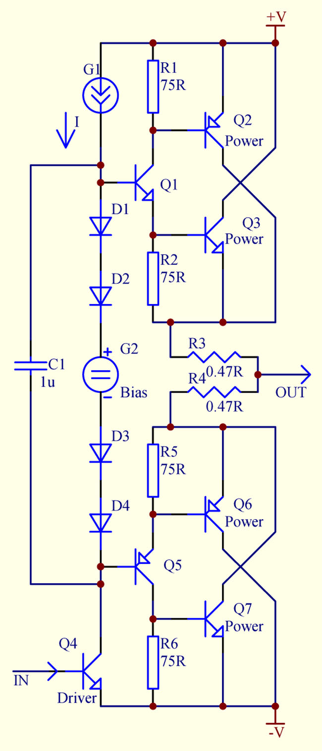
Fig. 3
Each leg has a phase splitting transistor, e.g., Q1 for the top side, which feeds both PNP and NPN power transistors, Q2 and Q3 respectively. The same current through the phase splitter drives both power devices Q2 and Q3. Output currents of Q2 and Q3 are added at the load, thus roughly doubling the output current in comparison with a conventional Darlington or Sziklai pair.
In other words, the circuit can be treated as a sum of a Darlington Q1Q3 and a Sziklai pair Q1Q2, sharing the same Q1 leading transistor. The net effective current gain B of such circuit is:
B = B1 * (B2 + B3)
The net beta is about two times higher than of a standard Darlington or Sziklai, which is an advantage.
The most important that the bottom "leg" has exactly the same current gain, because NPN and PNP output transistors also work together in parallel. Therefore, even if PNP and NPN betas are different, the sum of them are equal for both top and bottom leg. Thus the difference between the top and bottom legs now depends not on the output power devices, but on the phase splitters. Those splitters, being low power transistors, are easier to get matched. Also, because of the finite beta of the phase splitter, its emitter current is slightly better than the collector current. As a result, in the top leg NPN Q3 is getting a slightly better treatment, while in the bottom leg PNP Q6 is getting some "favour". However, since the beta of th phase splitter is large (100...200) this inequality is only within 0.5...1%. Further, if the splitter itself is made as a Darlington or Sziklai pair, this phenomenon will become absolutely negligible.
The similar approach can work for the MOSFETs:
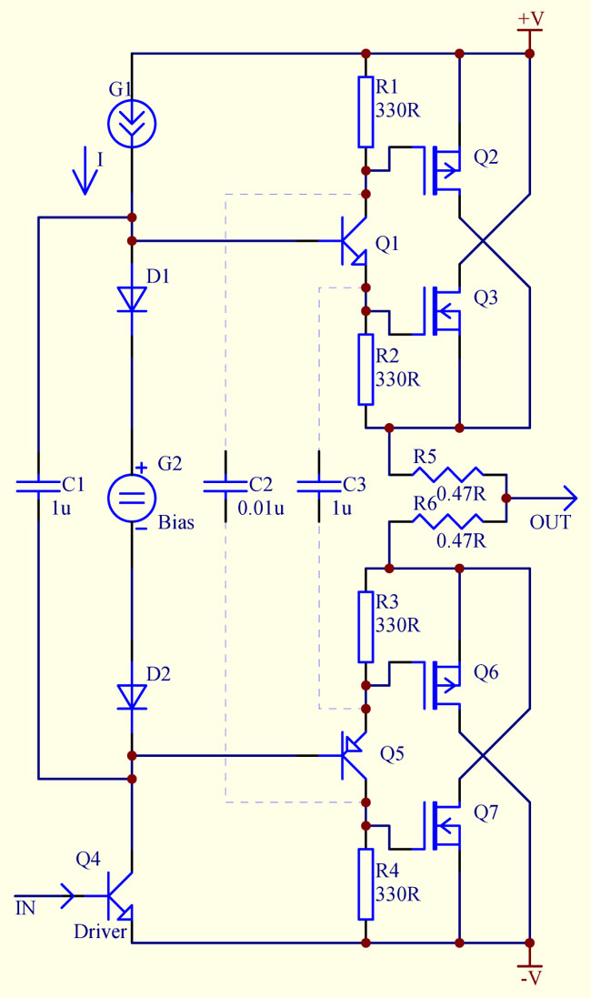
Fig. 4
Equal load resistors in each phase splitting transistor ensures equal drive voltage to the N and P-channel MOSFETs. It is the case for both top and bottom legs of the push-pull circuit. As a result, the effective net transconductance of the top and bottom leg is exactly the same, even if P-MOSFET and N-MOSFET have unequal transconductance.
The drawback of the MOSFET version (Fig. 4) is that because of possibly different threshold voltages of P-MOSFET and N-MOSFET, they cut off not at the same current, but typically P-MOSFET would cut off first, which results in a non-linearity at low currents. This might cause extra distortion in class AB operation, unless quiescent current is not increased accordingly. In class A operation this phenomenon might result in slightly underused output current range.
For the best dynamic performance, C2 and C3 can be added to the circuit. However, C2 can be used if the supply voltage rails are free from ripple and voltages are ramping slowly on power-up / power-down. Otherwise high shot-through currents may flow through Q2 / Q7 pair.
MOSFET version has a higher input impedance:
Zin = R2 * B1 * S * Rload, where
S -- transconductance of one MOSFET.
For example, with Rload = 8 Ohm, S = 1A/V, B1 = 100, R2 = 330 Ohm, input resistance Zin is about 250K.
BJT version (Fig. 3) would have
Zin = Rload * B1 * (B2 + B3).
With B2 = B3 = 40, Zin = 32K.
Thus, BJT version has less input resistance, which is not a great problem, as another follower stage can be added in front. An advantage of a BJT version is lower saturation, higher linearity and higher (closer to unity) voltage gain, which improves efficiency of the power stage. Generally, the BJT version is a preferred solution.
Note that the circuits presented above are simplified and for illustration only. To make the circuit more practical, gate protection Zeners and anti-parasitic oscillation stopper resistors might be added. In the MOSFET version, it is possible to avoid "inequality of treatment" (mentioned earlier) if the collector loads of the phase splitters (R1 and R4) are made slightly larger (by about 1/B1) than the emitter loads (R2 and R3). In order for N and P-channel MOSFETs to share the load more equally, possibly some small degeneration resistors should be added in series with the sources of the N-MOSFETs. Temperature compensation is shown only sketchy.