Introduction
High sensitivity diode envelope AM detector, able to linearly demodulate the smallest signals, has certain benefits:
- lower distortion at the troughs of deep modulation;
- less IF and/or RF gain is required before the detector;
- overall improved sensitivity of a radio, particularly of a crystal radio.
Choice of a diode for the best sensitivity
Which type of a diode is the best for achieving high sensitivity of an AM detector? Silicon diodes are usually criticised for their high 0.6V kink (threshold). Germanium diodes with low 0.15V kink are praised for their performance in crystal radios. Opinions vary about vacuum tube diodes. Some say they are perfect because they are slightly biased to conduction by thermionic emission even without signal. Others argue that the emission reverse biases the diode reducing its rectification efficiency and thus reducing detector sensitivity. Who is right and who is wrong? And what about Schottky diodes?
Obviously, kink voltage itself is not crucial for sensitivity of a diode detector, as the diode can be forward biased towards the "edge" of the kink. More important is the "steepness" or "sharpness" of the kink. It determines minimum voltage required to make a significant difference between diode current on "positive" and "negative" excursions of the input AC voltage.
For the initial, low-current part of current-voltage characteristic of a diode, which is relevant to sensitivity, current is approximately proportional to
exp ( Vf / Vt ), where: (1)
Vd - voltage across the diode (positive value for forward voltage);
Vt - thermal voltage, representing thermal energy of the electrons.
In turn, Vt = kT / q, where: (2)
k - Boltzman constant;
T - absolute temperature (degrees Kelvin);
q - charge of electron.
Exponential law (1) applies when charged particles (electrons), affected by thermal motion and external field, have to overcome some potential barrier (whether work-out function or Fermi level). This law (1) also applies to the initial part of the current-voltage curve of a vacuum diode. (At higher currents, the law of 3/2 takes over.) From (1) it follows that Vt defines the "steepness" of the exponent, and thus characterises the minimum voltage of efficient AC voltage rectification.
For room temperature (T=300K) at which semiconductor diodes operate Vt = 25...26mV. For the tubes with oxide cathode (T=1200K) Vt=100mV.
We can say that an AM detector based on a semiconductor diode operates well above 25mV, while a vacuum tube detector needs at least about 100mV for good linear operation.
CONCLUSION: Tubed AM detector is four times less sensitive than a semiconductor diode (crystal) detector. Semiconductors win, valves lose. Vacuum diode AM detector sensitivity can be somewhat improved by running the cathode cooler, at a reduced heater voltage. Such trick is done, for example, in HCR-62 communications receiver.
AM detector bias optimisation
More accurate equation defining current-voltage characteristics of a semiconductor diode is:
Id = Io * (exp (Vd / Vt) - 1), where (3)
Id - current through the diode (positive value for forward current);
Io - reverse (saturation, leakage) current of the diode.
From this equation it follows that at very low voltages (below approximately 5mV) a diode behaves as a resistor with equivalent (differential) resistance Rd:
Rd = Vt / (Io + Id). (4)
Usually this rule is spelled out like: "Differential resistance of an ideal diode is 25 Ohm at 1mA of forward current." This rule is true for relatively large currents, but for very low currents typical for small signal detector operation, reverse saturation current Io (as per equation (4)) shall be taken into account too.
For example, differential resistance of a Germanium diode with reverse current of 1uA will be about 25KOhm even without any bias current.
A generalised AM detector circuit is presented in Fig. 1.
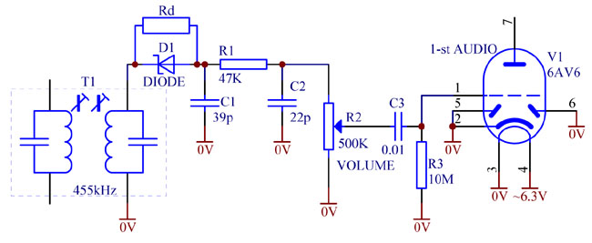
Fig. 1. AM detector circuit. Rd - differential resistance of the detector diode.
Note first of all that it is recommenced to use volume control potentiometer as the detector load. Such configuration allows to handle deeper modulation without distortion.
It is well known that for a large signal, equivalent load which a diode detector presents to the source (an IF transformer in this case) is Rload / 2.
For very small signal, say under 5mV, the equivalent load on the IF transformer is obviously Rd, as the impedance of C1 is relatively small.
It is logical to assume that for the "smooth" operation of the circuit, it is desirable to have equivalent load on the source constant regardless of the signal amplitude. Therefore a diode shall have such bias and/or such reverse current Io so that its differential resistance Rd equals half of the load resistance.
Rd = Rload / 2 (5)
In this particular circuit, Rd shall equal about 270K (R1 is a part of Rload). This in turn requires that the sum of forward bias current (at zero signal) and the reverse leakage current equals about 90nA.
Since there is no bias provision in the circuit, the only way to achieve Rd = 270K is to select a diode with the reverse current of about 90nA at room temperature. Such diode would be a Schottky diode, probably BAT46 or similar. If Io < 90nA, the diode will not conduct well at low signal (kink voltage will be too high). If Io > 90nA the diode will conduct, but it will be also shunting/loading the LC tank unnecessarily with its low Rd. In both cases sensitivity of the detector will be compromised. Only with Rd = Rload/2, the best sensitivity of about 25mV can be achieved.
The following guidelines apply:
1) Silicon diodes have negligible reverse current Io and will require forward bias which will be described below.
2) Schottky diodes like BAT46 with Io = 50...80nA can be used in valve radios where detector load is of the order of 500K.
3) Germanium diodes with Io=0.5...1uA have Rd of 25...50KOhm respectively and are not suitable for valve radios. However, they are suitable for crystal radios working onto high-impedance headphones. Note that several diodes can be connected in parallel to increase the total Io.
Usually diodes rated for higher forward current and lower reverse voltage would have higher Io and lower Rd. For example Schottky diode BAT85 has about Io = 300...400nA.
Surface mount Schottky diodes like BAS40, BAS70 may be useful too. Schottky diode 1N5711 has a very low capacitance (under 1pF, but with low Io=5...15nA needs forward bias even in high impedance detectors.
Note that Io is not temperature stable and doubles for every 10 degrees Celsius. Therefore the diodes must be protected from the heat, otherwise lowering Rd will start "killing" sensitivity. In theory it is possible to place the diodes in a thermostat to heat (or even cool by Peltier cells for better sensitivity) to maintain optimum Rd, but such exotic solutions are not discussed here.
Much more practical is to use silicon p-n diodes with negligible Io as detectors and apply temperature compensated forward bias to build up required Rd, as shown in Fig. 2.
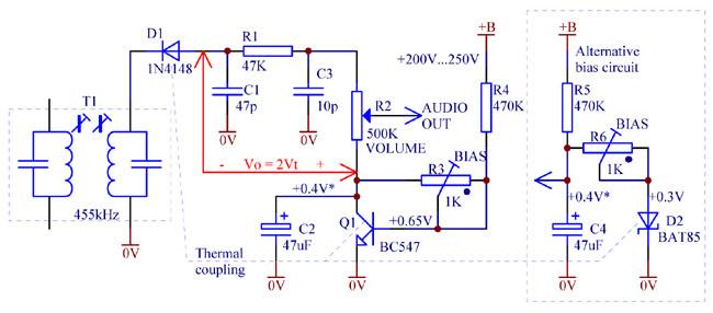
Fig. 2. AM detector with temperature compensated forward bias.
Usually 0.3...0.4V of bias is needed for a high impedance detector. This bias voltage shall have the same --2mV/degreeC temperature coefficient typical for a diode. Two alternative methods of creating bias voltage are recommended as shown in Fig.2.:
a) Subtract some fixed voltage (developed across potentiometer R3) from temperature dependent transistor Q1 base-emitter voltage;
b) Add some fixed voltage (developed across R6) to the temperature dependent low voltage drop of a "large" Schottky diode D2.
Temperature compensating elements Q1 or D2 shall be thermally coupled (glued) to the detector diode D1 and kept away from heat sources.
From equations (4) and (5) if follows that to achieve Rd=Rload/2, optimum bias current should equal:
Id = 2*Vt / Rload;
In other words, when bias current is optimum, it will create a voltage drop Vo = 2*Vt across the detector load (at no signal condition). Thus, one way of optimising the bias is to adjust R3 (or R6) to get about 50mV across the load (R1 + R2).
DETECTOR OPTIMUM BIAS RULE
For a low leakage diode, under no signal, bias current shall produce 2*Vt voltage across detector load: 50mV for a p-n diode, 200mV for a vacuum diode.
When using a multimeter for checking this voltage, diode D1 must be temporarily shunted by a large capacitor (0.47uF) to prevent rectification of noise and hum picked up by the multimeter leads.
Alternatively, the bias can be adjusted to for maximum sensitivity of the detector. Receiver antenna should be disconnected, RF GAIN control, if present, set to minimum (or mixer tube pulled out), AF volume set to maximum to get just barely audible static noise. Then adjust bias (R3 or R6) to maximise the audible noise.
Optimally biased AM detector is very linear down to the smallest signal (25mV) and therefore works with minimum distortion and handles deep troughs of modulation. Audio quality significantly improves.
To prove the point, Fig. 3 illustrates a modification of 9R-59DS communication receiver, where a biased AM detector and efficient AGC are introduced.
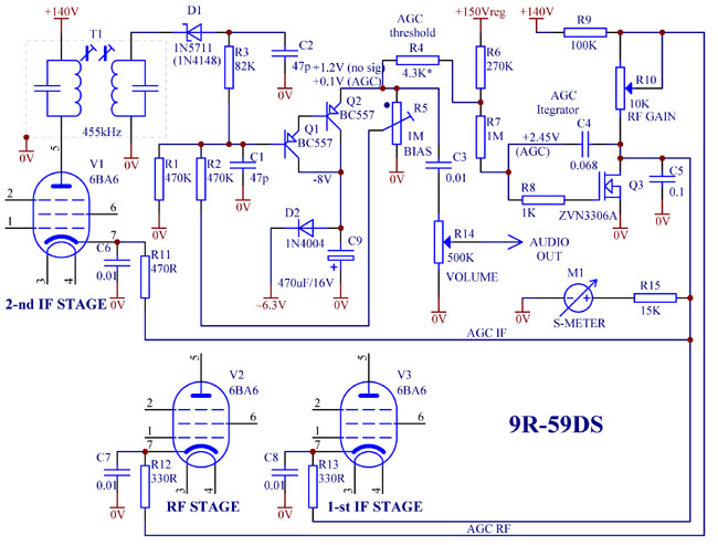
Fig. 3. Optimised AM detector and AGC in 9R-59DS.
In the modified circuit, AM detector is not shunted by a noise limiter, AGC filter, volume control or other loads. Instead it is buffered by a Q1Q2 Darlington for the best handling of deep modulation. Voltage drop from this Darlington, adjusted by R5 is used as a bias to the detector diode D1. AGC topology is completely changed. Instead of using negative AGC voltage to the tube grids, positive voltage is applied to their cathodes. MOSFET Q3 works as an integrator, R7C4 determining its time constant. Parasitics stopper resistor R8 is essential. Voltage drop over R4 is set to approximately equal threshold voltage of MOSFET Q3. This with no signal, Q3 is fully conducting, driving the tubes to full current. With a signal, AM detector diode develops a negative voltage which eventually pulls top end of R7 below the MOSFET threshold, Q3 starts to close, cathode voltage raising, shutting the tubes. Because of a very high gain of the MOSFET, AGC maintains almost constant IF level on the detector.
In this circuit there is no obvious way to measure voltage drop on the detector load, so bias optimisation can be done only by the "faint noise peaking" technique.
Crystal radio detector biasing
A generalised crystal radio circuit is shown in Fig. 4.
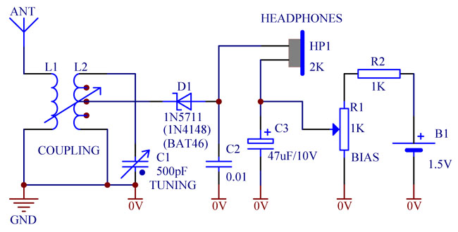
Fig. 4. Crystal radio with detector diode bias
By changing coupling and using different taps on the coil, a trade-off between selectivity and received sound volume is made. Bias is supplied from a battery cell B1 and adjusted by R1 for maximum volume and more importantly, minimum distortion of the sound. Optimum Rd of the diode in such circuit is expected around 2...8KOhm depending on the headphones used. Even a germanium diode would need some forward bias to achieve such a low Rd, let alone Schottky or silicon p-n diodes.
Regenerative radio
A generalised schematic diagram of a regenerative radio is shown in Fig. 5.
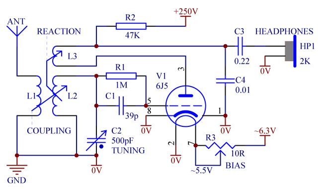
Fig. 5. Regenerative radio with cathode temperature optimisation
Is it true that a regenerative radio is more sensitive than a passive crystal radio? Yes and no. Of course, a tube provides both RF gain by Q-multiplication and also audio gain of the grid-detected signal. However, a grid detector itself is far less efficient than a crystal (semiconductor diode) AM detector. As mentioned above, Firstly, Vt for a tube is about 100mV as opposed to 25mV for a semiconductor. So, a tube is less sensitive and needs about 100mV of RF on its grid to produce reasonably clean sound, while a p-n diode needs only 25mV. Secondly, a grid detector is usually overbiased and is not biased optimally. It became a custom to select quite large values of "grid leak" resistors (R1 in Fig.5). A large grid leak resistor ensure low loading of the LC tank, and hence more sensitivity, but here is a problem. Ideally, voltage drop across a grid leak R1 shall be about 2*Vt = 200mV as discussed above. In practice, however, for the modern tubes with close grid-to-cathode spacing, electron emission easily develops 500...1000mV of the negative bias on the grid. Needless to say, such overbiased grid detector further degrades sensitivity and works with significant distortion.
A remedy (apart from reducing R1) is to reduce cathode temperature. A rheostat R3 is used for that purpose. To avoid cathode poisoning, cathode temperature shall not be reduced too much. Heater voltage reduction from 6.3V to about 5V already reduces distortion while a tube continues to operate stably..
Crystal regenerative radio
It is tempting to combine high sensitivity and low distortion of a crystal detector with amplification benefits of a regenerator. In fact, it is possible, as per Fig. 6.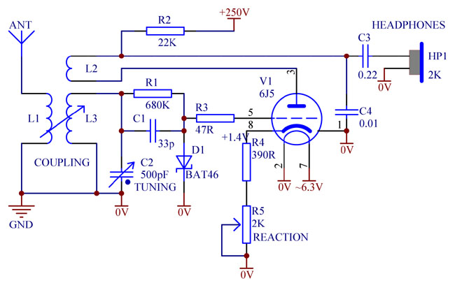
Fig. 6. Crystal regenerative radio
As can be seen from the circuit diagram, AM demodulation function is taken away from the tube and given to a Schottky diode D1. The semiconductor diode is four times more sensitive than a tube. The triode still does Q-multiplication and audio amplification, but not demodulation. It is negatively biased by the cathode resistors biased (by 1.4V or more) to prevent any undesirable grid current affecting the detector diode D1. A grid stopper R3 is not essential, but is recommended as a precaution.
Modifying a regenerative radio from Fig. 5 to Fig. 6 gives a dramatic improvement in sound quality and sensitivity. Now the radio effectively works with four times smaller signal levels which further reduces distortion and requires less regeneration (reaction). With a ferrite rod antenna only and with little regeneration, such radio receives a dozen of local AM stations. Linearity of the triode is enhanced by local negative feedback through R4 and R5. A drawback of this circuit though -- need to select diode D1 for a proper Io (50...60nA in this particular case). If Rd drops below R1 / 2 (as a result of say warming up) then reaction control can become coarse and "hysteretic". Therefore it is recommended to select the diode with Io of 20...30nA -- slightly lower than optimum.
To overcome this issue, another version of a crystal-regenerator hybrid is offered, see Fig. 7.
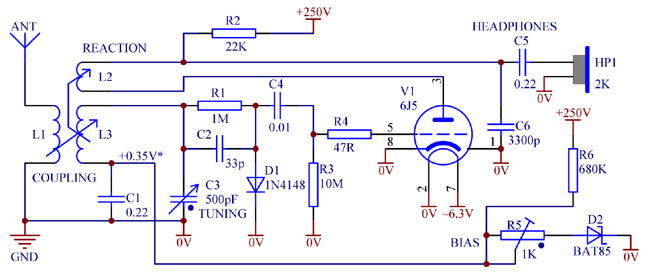
Fig. 7. Temperature compensated crystal-regenerative radio
In this circuit, bias applied to a silicon p-n diode D1, is temperature compensated by D2. By adjusting R5, the bias can be optimised for minimum distortion, maximum volume or for the "softest" regeneration. Grid current of the tube (which biases it) is completely decoupled from the detector by a blocking capacitor C4.
Note that the circuits in Fig. 6 and Fig. 7 are given as examples. Circuit ideas from both of them can be combined or intermixed.
Interestingly, in the 30's of the last century smart German engineers realised the benefit of separating detection and regeneration/amplification functions and used this principle in the commercial receiver Lorenz 100W, launched in 1937 (Fig. 7A). A dedicated diode works more efficiently than a cathode-grid interval, and a separate reversely biased amplifier/regenerator tube AF7 produces less distortion than a conventional grid-leak detector.
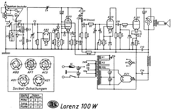
Fig. 7A. Schematic diagram of Lorenz 100W radio (1937) with separate detector and regenerator.
In retrospect, it would have worked even better if the diode detector valve AB2 had been running at a lowered heater voltage. Needless to say, a modern silicon or Schottky diode gives far better sensitivity.
Measuring reverse current Io of a diode
Reverse current Io value is crucial for selecting Schottky and Germanium diodes for unbiased applications. Io can be assessed by several methods.
1) Measure Rd with an ohmmeter. On a high-ohm range of a multimeter try to measure resistance of a diode in forward and reverse connection. Choose a range where both readings are of the same order of magnitude, then average them. This is a crude method for a rough direct estimation of Rd. It is most suitable for Germanium and larger Schottky diodes.
2) Measure reverse current. You do not need a microammeter. Switch your multimeter into a DC voltage mode and connect to a 1.5V or 3V battery via a reverse connected diode. The internal impedance of the multimeter will work as a current sensing resistor. Cheapest hand-held multimeters usually have 1M resistance, and thus will give 1nA/mV reading. A bit more expensive multimeters have 10M resistance and will be giving 100pA/mV or 1nA/10mV. You need to know resistance of your multimeter. To find out, the easiest way is to measure voltage of a battery via a series 1M resistor. If the reading is 50% of the known battery voltage, then the multimeter has 1M resistance. If the reading is only 10% lower than the actual battery voltage, then your multimeter has 10M resistance.
3) Calculate Io from diode forward voltage drop. Pass a known current Id of about 1uA through a diode under test in forward direction, for example from a 9V battery via a 8.2M resistor. Measure forward voltage drop. From the exponential equation (3) estimate Io. Roughly assume that every 60mV of forward voltage means that Io is 10 times smaller than Id, and each 30mV of forward voltage mean that Io is 3 times smaller. For example, suppose you measured 100mV of voltage drop. 100mV can be represented as a sum of 60mV + 30mV + 10mV. Respectively, Io is 10 times smaller than Id, then another 3 times smaller and then roughly 1.5 times smaller still. Thus, Io = 1uA / (10 * 3 * 1.5) = 1uA / 45 = 22nA.
Silicon p-n diodes do not need any Io measurements as Io is very small. Such diodes always need forward biasing, which can be adjusted by "50mV on the load" rule or for the best sensitivity to the smallest signals.