Zener diode or cold-cathode glow gas discharge tube?
Voltage regulation (stabilisation) is very important in tube vintage equipment. Supply voltage regulation improves stability of the test gear, such as audio and RF oscillators, tube voltmeters, distortion meters, to name a few. It is a must for a decent communications receiver -- to reduce frequency drift. Even in audio amplifiers voltage regulation will not hurt, completely eliminating hum and transients possibly caused by mains voltage fluctuations.
If a piece of vintage equipment does not have a voltage regulator, it might be a good idea to retrofit a simple shunt voltage regulator it in the course of upgrade. But which type of a regulator to choose -- high voltage Zener diode or a glow gas discharge tube?
A high voltage Zener diode (which is actually not a Zener diode but an avalanche breakdown diode) seems like a good modern solution, but it has problems. Firstly, though some of the Zeners are rated at 5W, it is doubtful that it can withstand such dissipation for long time if not soldered to large copper plated areas. Attaching a heatsink or clamping such axial cylindrical part to chassis is inconvenient. But a far more serious problem is excessive noise of an avalanche (Zener) diode.
Avalanche (Zener) diode noise
A simple circuit can be used to evaluate a shunt regulator noise (Fig. 1).

Fig. 1. Shunt voltage regulator (Zener or glow discharge tube) noise test circuit.
A 160V 5W regulator diode 1N5384BG was tested with R1 = 100K, Cr = 100pF (oscilloscope probe capacitance only) at Ir = 70uA current. The result was quite shocking (Fig. 2).
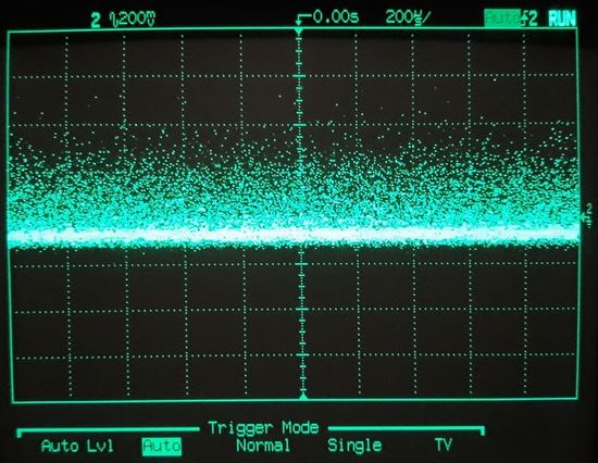
Fig. 2. Noise of 1N5384 high-voltage Zener at 300uA, not filtered.
Enormous peak-to-peak noise exceeded 600mV which is far more than ordinary shot noise would have produced. Noise distribution looked asymmetrical, with the bottom envelope more or less regular, while the top one was extremely "loose" and "random".
Zooming in by faster oscilloscope time base and triggering on the extremes, it became obvious that current through the avalanche (Zener) diode does not flow continuously, but rather consists of isolated "discharges" (Fig. 3).
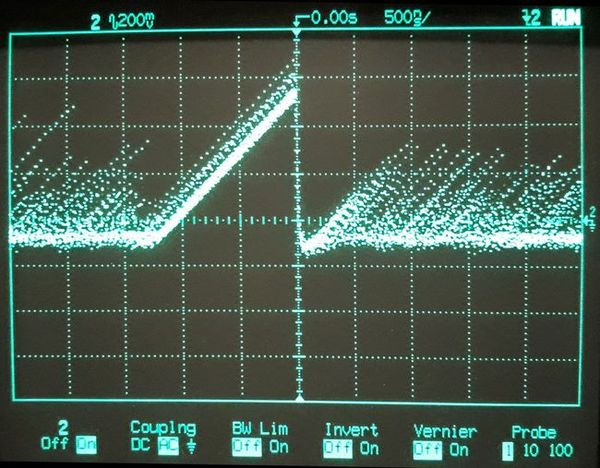
Fig. 3. A typical single avalanche breakdown micro-event in a Zener diode.
One of such discharges is captured in Fig. 3. For as long as 1.3us current is not flowing at all, voltage linearly ramping up. (Effective capacitance, including the probe is about 150pF.) Then at a certain moment breakdown happens and voltage is quickly (fall time is about 30...50ns) drops to some quite well defined level. From then on, current stops flowing and the process repeats until the next breakdown happens. Apparently, each micro-breakdown occurs not when voltage reaches some particular threshold, but rather randomly, depending on thermal excitation of the atoms. In a way, such avalanche diode operates as a random relaxation oscillator. Physics of this process is described here. Needless to say, how damaging such noise might become if such voltage regulator or its wiring is located close to sensitive RF circuits of a radio receiver.
Shunting the diode with a capacitor changes the picture, but not the relaxation oscillation nature (Fig. 4).
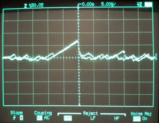
Fig. 4. Avalanche micro-breakdown of a Zener diode shunted by 0.01uF capacitor (Ir = 70uA).
Shunt capacitor Cr = 0.01uF reduces noise to 70mV pak-to-peak. Time between micro-discharges increases, reaching 10us in this example (Fig. 4). Fall (discharge) time is about 500ns in this case, which translates to about 50 Ohm Zener "internal resistance" during a micro-discharge. Therefore, instantaneous micro-discharge current reaches 1.4mA -- 20 times larger than average Zener current. It is obvious that such pulsed noise is quite "aggressive" as it may create magnetic interference, radiated by the wiring.
With current increasing, Zener diode voltage noise reduces (Fig.5).
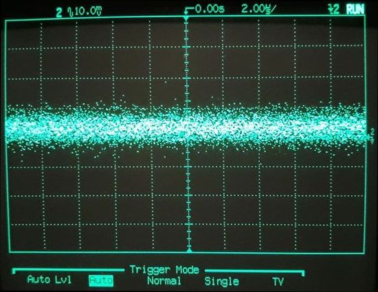
Fig. 5. Voltage noise of 1N5384BG Zener diode at 25mA without shunting capacitor.
In the example, peak-to-peak noise is about 20...25mV at 25mA, which is still far more than common electron flow shot noise could have produced. At a higher current, individual micro-discharge events become more frequent, rise time becomes shorter than fall time, so the discharge events in different parts of the p-n junction overlap and blend together creating an impression of a normal Gaussian noise. Still there is a reason to believe that each micro-discharge can dump anything from zero up to 3mA of current in 30ns or so. Average frequency of such events can goes into Gigahetz region. Because of the low avalanche diode impedance, 0.01uF shunting capacitor would not significantly reduce noise voltage, only perhaps by about 50%. Thus an avalanche (Zener) diode represents an obnoxious low impedance wide-band voltage noise source. Therefore, special attention is needed to fully contain and isolate it (Fig. 6).
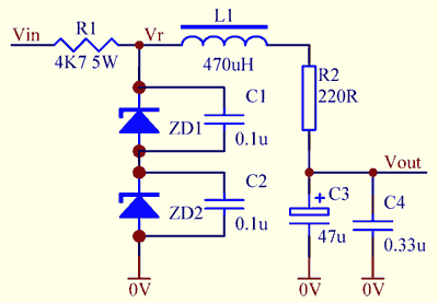
Fig. 6. Zener diode noise filtering.
As shown in Fig. 6, each Zener diode (if several are connected in series for higher voltage) should be individually shunted by low inductance ceramic or film capacitors (C1 and C2 in Fig. 6), soldered as close as practical to the diode body and with shortest possible leads. This technique will help reducing noise current circulation loop area and thus help minimise magnetic noise radiation. A large electrolytic filtering capacitor C3 can not be directly soldered to the Zener and inevitably has be placed some distance away. To prevent noise currents flowing into it, filtering impedance L1 and/or R2 should be inserted. Furthermore, node "Vr" shall be wired tightly (in other words, R1, L1, R2 physically close to the Zeners with short wiring) in order to minimise electric field radiation from "Vr" circuit. Lastly, it is sensible to place the whole assembly away from sensitive RF circuits.
So this seemingly "trivial" task of regulating high voltage with Zeners, if dealt with thoroughly, becomes quite involved. Besides, due to R2, load regulation may be less than ideal... In view of the above, it is becoming obvious that Zener solution is not perfect, and it is worthwhile revisiting and reconsidering old glow gas discharge voltage regulator technology as an alternative.
Glow gas discharge voltage regulator noise
Testing 0C3 (VR105/30) glow discharge regulator tube in the circuit Fig. 1 with R1 = 1K and Ir = 25mA produces the following picture (Fig. 7).
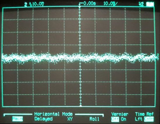
Fig. 7. Voltage noise of 0C3 105V glow discharge voltage regulator with R1 = 1K and Ir = 25mA, Cr = 0.
Peak-to-peak noise is only 3...4mV without any filtering shunting capacitor -- at least five times better than of a Zener diode. (Small 100Hz ripple is caused by finite line regulation.) Not only the noise is smaller than of a Zener, it is "softer" as well -- at high frequencies a glow discharge tube represents a constant current source or perhaps a resistor, or a combination of the above, while at low frequencies it behaves as a low impedance voltage source. This phenomenon of inductive impedance of a glow discharge voltage regulator above 6kHz, explained by a relatively slow ionization/recombination process, was studied as early as 1949 - 1954. Thus "sluggishness" of glow discharge is a benefit, which makes possible to practically eliminate high frequency noise by a relatively small (0.01uF) shunting capacitor.
Voltage regulation and intricacies of glow discharge
In a shunt regulator, differential impedance (Zd) determines quality of both line and load regulation. Ideally Zd shall be zero. To assess it, a simple test circuit (Fig. 8) was built to "exercise" a regulating element over 0...40mA current range and record corresponding voltage variations in a form of X-Y plot, or rather I-V plot in this case.
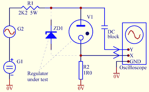
Fig. 8. Testing voltage vs current characteristic of a regulator element.
1N5384 Zener avalanche diode gave the following picture (Fig. 9).
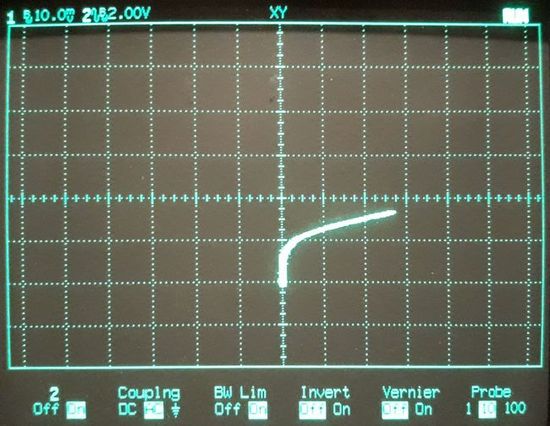
Fig. 9. I-V plot of a 160V Zener diode 1N5384. Horizontal scale -- 10mA/division; vertical scale -- 2V/division.
The curve looks classic. Differential impedance Zd is about 60 Ohm above 5mA. Note that the curve is not logarithmic as I-V curve of a forward biased p-n junction would have been, but appears to have a linear "tail". Note that differential impedance Zd does not fall with current rising, and therefore running unnecessarily high current through the diode will not improve voltage regulation, and might even degrade it due to a smaller ballast resistor R1 and higher temperature rise.
In comparison, cold-cathode glow discharge voltage regulators all behave differently, as illustrated by the plots below.
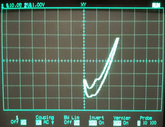
Fig. 10. 0A2 cold cathode regulator I-V plot. Horizontal scale -- 10mA/division; vertical -- 1V/division.
At low current, approximately from 1mA to 5mA, 7-pin miniature 150V glow regulator 0A2 shows negative differential impedance of --200 Ohm. At higher current Zd is about +250 Ohm. It also exhibits hysteresis -- regulated voltage may differ by up to 1V depending whether current is rising or falling. Definitely this tube is inferior to a Zener in terms of voltage regulation. Note that in this experiment (as well as in the next two pictures) grow discharge was not allowed to extinguish -- current did not fall below 1mA. Current-voltage cycling was sinusoidal at 20Hz -- frequency low enough, so that the picture is not affected by the delay of ionisation/recombination process.
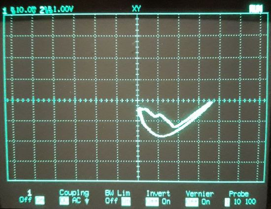
Fig. 11. VR105/30 I-V plot. Horizontal scale -- 10mA/division; vertical -- 1V/division.
A bigger octal VR105/30 (0C3) regulator tube gives Zd about --100 Ohm below 20mA and +100 Ohm above 20mA, and a similar 1V hysteresis. Regulation performance is comparable to 1N5384 Zener.
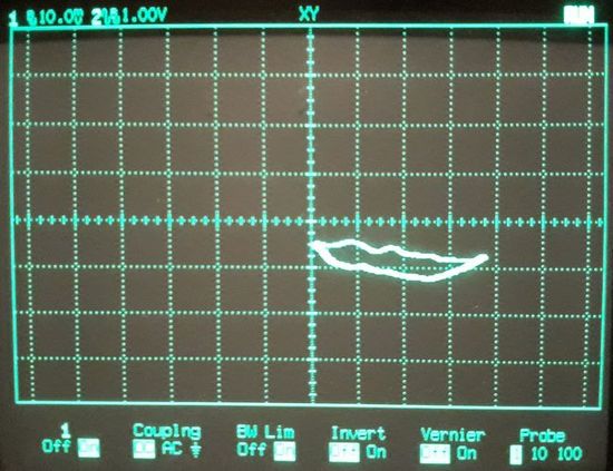
Fig. 12. 0C3 I-V plot. Horizontal scale -- 10mA/division; vertical -- 1V/division.
Another sample of an octal 0C3 tube from a different manufacturer, demonstrated far better regulation -- Zd is a s low as --20 Ohm up to 30mA and +30 Ohm close to the maximum rated current. Hysteresis and overall regulation is quite tight -- about 0.7V. Surprisingly, performance of this particular sample of an old cold cathode voltage regulator from the 1950's exceeds the results of a contemporary Zener diode (Fig. 9).
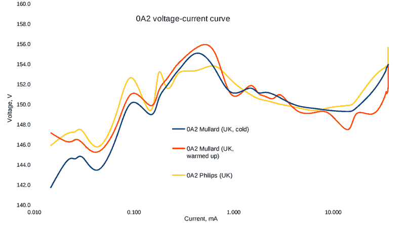
As can be seen from the above three plots, voltage changes in a glow tube are non-monotonic -- it goes through peaks and troughs. Accordingly, differential impedance changes sign from positive to negative. Such phenomenon, as well as hysteresis, deserve some elaboration. The following two graphs, Fig. 13 and Fig. 14, show detailed graphs of sustaining voltage versus current for several samples of glow discharge voltage regulator tubes.
|
|
Fig. 13. I-V graphs for several samples of 0A2 voltage regulator tube.
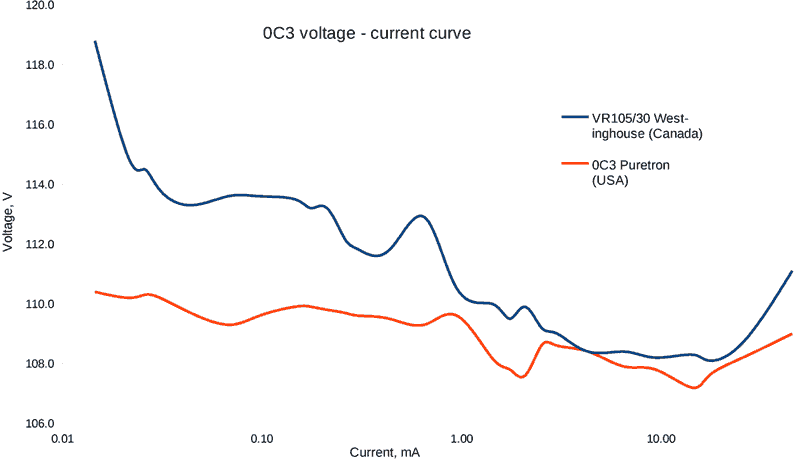 |
Fig. 14. I-V graphs for several samples of 0C3 (VR105/30) voltage regulator tube.
To understand this intricate behaviour, one need to know that glow discharge is sustained by secondary electron emission when cold cathode is bombarded by positive ions (or neutral atoms, accelerated by earlier impacts of the ions). In turn, effectiveness of the secondary emission depends on the work function of cathode material. In other words, it depends on the chemistry of cathode coating or cathode contamination. Finally, area of cathode glow is proportional to the current through the tube.
At a very low current glow discharge starts at the tip of the striker (starter) electrode. It is a pin spot-welder radially on the inside of the cathode cylinder and reaching within a couple of millimetres of the central anode rod. As the current increases, cathode glow spreads down the striking electrode and at about 0.6mA entirely envelops it. When the glow spot reaches the base of the pin where it joins the cathode, glow "jumps" off the pin onto the cathode. With current further increasing, the glow spot expands in size. At the same time it might start moving, "crawling", wandering or "flickering" around the cathode surface.
There exists a fundamental principle that a physical system tends to assume a state with the lowest energy. Glow discharge is not an exception. As the glow spot is growing, if emission conditions at some section of its boundary turn out to be better than in its recent position, the discharge would jump or "slither" into that new location where work function is at least a little lower. Thus the glow spot is always on the lookout for the (relatively) best local emissive position. It would stay "anchored" to the (locally) best position until, while the spot is expanding, it comes across a better one and jumps into it. So, while the glow is sitting in the fixed spot and growing, discharge voltage is growing too -- differential impedance Zd is positive. Each incremental jump to a slightly "greener pasture" translates into a corresponding incremental drop of regulated voltage. Thus the I-V curve consists of succession of peaks and troughs (Fig. 13, 14). General trend is downwards (negative impedance) as every next "better" local spot requires less and less energy (and hence voltage) for sustaining sufficient secondary emission. On the "dynamic" I-V plots (Fig. 10 - 12) glow spot growing and then jumping behaviour is reflected by bumps and undulations of the upper trace, while the overall trend is downward.
Once regulator tube current reaches about half of the maximum rated current, or in other words, once the area of the glow spot has reached or exceeded half of the available cathode area, all the local "best spots", most likely, have been "explored" and "taken" by the glow. Now the glow is sitting anchored in the absolute best spot -- global minumum of the emission work function. If, with further increasing current, the glow spot continues to expand, it will not encounter any better location. There is no "incentive" to jump anywhere, as everywhere else emission conditions could only be worse than in the existing location. As a result, regulated voltage steadily increases. It can be clearly seen in every I-V plot above -- a final (high current) part of the "tail" is always positively directed (Zd is positive) and free of any humps and bumps.
Note that for some glow discharge regulators the "tail" of the V-I curve with consistently positive Zd begins as early as at 30...40% of maximum current rating, while for others begins only at 3/4 of the rating. It all depends on uniformity of cathode emissive coating, precision of the electrode assembly and amount of cathode surface contamination. If the cathode is well made and uniform, most of its area would have equally good emission, and quality regulation with low Zd will continue almost to the maximum rated current. If, on the other hand, the cathode is bumpy, blemished by spot welding, contaminated or poisoned by non-emissive oxides, then only its small part is effectively usable and able to produce stable regulated voltage. Beyond that limited area emission is difficult or impossible, the tail steeply goes upward and regulation performance suffers. Therefore, it is sensible, if possible, to run glow discharge tubes under 50% of their maximum current ratings.
Some voltage regulators tend to flicker (glow patch jumping back and forth between two spots), why others do not. What does that mean? Flicker happens if several adjacent areas of the cathode have almost identical emission potential. Then every minutest fluctuation might get the glow slither from one spot to the other and back. Therefore, it may be inferred that a flickering regulator tube most likely has a very uniform cathode and most likely would produce tight regulation over a wide current range. However, every flicker event causes in a small -- several millivolts -- regulation voltage fluctuation. Steadily glowing tube, to the contrary, likely to have non-uniform cathode emission with a few localised "sweet spots", in which the glow tends to sit anchored. Expansion of the glow beyond these spots results in voltage rising and hence poorer regulation -- long "tail", large positive Zd, wide hysteresis "eye". In this respect, behaviour can vary from tube to tube, manufacturer to manufacturer and change over the tube life span.
Though explained above in detail, behaviour of a particular tube is impossible to predict by looking at a cold tube or its datasheet. Testing of each species according to Fig. 8 may be impractical. So, observing flicker might give some hint to quality of regulation to expect. If absolute line regulation over wide range of supply voltage is of primary importance, then flickering species should be preferred. Such would outperform Zeners in terms of line and load regulation. If line regulation is of no importance, but minute random voltage fluctuations are strictly not welcome, then plug a steadily glowing sample in the socket, or use Zeners.
So far, glow discharge habits have been examined with current rising. When it starts to fall, the picture is different -- the voltage trace is always lower, in other words, hysteresis can be observed (Fig. 10 - 12). This is also easily explainable. When current is ramping up, the glow spot makes several jumps through several local minima until it ends up in the global minimum -- absolutely best spot with the lowest voltage. When current is ramping down, the glow is already sitting in the best spot and is not going to give it up retracing the path to it. Instead the glow would hold on to this best spot obviously producing the lowest possible voltage. Only when current reduces to about 500uA or so, and the glow shrinks to a tiny patch of about 1mm in size, only then it might become unstable, unsustainable and, due to some environment fluctuations, extinguish itself. Then the discharge would usually re-ignite back at the striking pin, and voltage would jump back to the initial relatively high value. Then the whole process may repeat. Again, "flickering" voltage regulators with more uniform cathode tend to have less hysteresis, as the difference between local and global minima is smaller.
In conclusion, in spite of quite queer behaviour, cold cathode glow discharge technology is capable of delivering reasonably good voltage regulation. Certain ("flickering") species can provide lower differential impedance and hence better line regulation than avalanche diodes (Zeners).
Improvements to a glow discharge voltage regulator
Though greatly outperforming an avalanche diode (Zener) in respect of noise and being in par or sometimes better in terms of voltage regulation, a conventional glow discharge stabiliser has its own issues. They are caused by striking voltage of a glow tube being higher than burning discharge sustaining (burning) voltage. A basic glow discharge shunt voltage regulator circuit is presented in Fig. 15.

Fig. 15. Basic glow tube voltage regulator.
It is not permissible to connect a large capacitor, more than 0.1uF, directly across the glow tube. If a capacitor (C2) were connected directly, then, once discharge has ignited, the tube would try to bring Vr back down to maintaining (sustaining, regulated) voltage by quickly discharging C2. Instantaneous current and instantaneous power dissipation would spike. Localised gas and/or electrode temperature raise would create extra thermionic emission or ionisation, and the discharge would turn from glow into an arc, discharging the capacitor further to 10...20V. Such process, literally vaporising electrode metal, is damaging to the tube.
To prevent collapsing into arc mode, a current limiting resistor (R2) is usually inserted between a tube V1 and filtering capacitor C2. According to the specifications of the common regulator tubes, maximum difference between striking and sustaining voltage is 20...25V. Maximum safe intermittent current is 100mA for octal voltage regulator tubes as 0A3, 0C3, etc., and 75mA for 7-pin miniature types 0A2, 0B2, etc. Therefore, minimum value of the current limiting resistor R2 is 220...330 Ohm respectively. Though, according to datasheets, C1 shall not exceed 0.1uF, it would be safer to use a smaller value, like 0.01uF, taking into account that post-ignition current spike through R2 is already close to its specified maximum. Loss of 5...10V across R2 and consequent degradation of load regulation are obvious shortcomings of the basic circuit (Fig. 8).
However, a simple modification (Fig. 16) can help overcome these drawbacks.

Fig. 16. Decoupling of filter capacitor by a diode.
When Vr drops after igniting, decoupling diode D1 prevents the glow tube from force-discharging filter capacitor C2. Hence, glow tube V1 is not subject to any current stress at all, no matter how large C2 may be. Capacitor C2 would then slowly discharge through the load until Vout settles at Vr - 0.7V. This simple, yet little known improvement allows to eliminate undesirable voltage loss, achieve excellent load regulation (as good as the "naked" tube can provide) and allow to perfectly filter low-frequency fluctuations and hum by using a large C2 (together with C1 which would take care of high-frequency noise).
Another problem remains though. During a power brown-out, when Vin drops below normal operational limit, regulator tube might extinguish. If after that power supply is restored, but hovering at the lower limit, and the load drawing its nominal current, the regulator tube might not re-ignite. This is particularly likely for an aged tube with elevated striking voltage. As a result, the load might be getting excessive and unregulated voltage until the glow tube re-ignites. Such situation is undesirable. To avoid that from happening, ballast resistor R1 is always selected lower than would be sufficient for a steady state operation (after V1 has ignited with all other tubes in the equipment cold). Lower than necessary R1 value causes unnecessary power and heat dissipation in the equipment. How wonderful it would be, if a glow tube were not allowed to completely extinguish during brown-out and were always ready for action. Fortunately, such feature is also easy to introduce (Fig. 17).
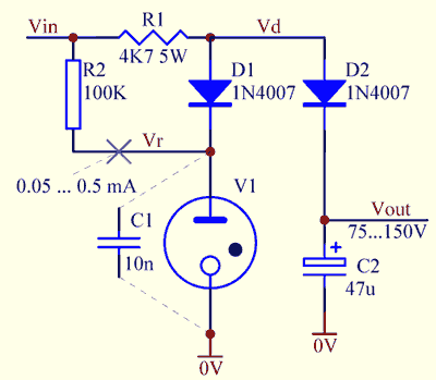
Fig. 17. Non-extinguishable glow discharge voltage regulator.
Diode D2 is inserted between the glow regulator and load node Vd. at the same time, small current is fed to the tube directly from the power supply. As a result, even when Vd is driven below sustaining voltage, some minor glow will remain due to current through R2 (assuming Vin does not fall below striking voltage). Only relatively small current of 0.05...1mA is needed to avoid total extinguishing of the tube. Such current is enough to keep this king of "pre-glow" -- glow on the striker (starter) pin. Once Vin restores to normal level, the discharge quickly jumps off the starter pin onto cathode. Though transition from the "pre-glow" to normal operation would typically involve 1...2V voltage drop, it is nowhere as much as 5...25V difference between sustaining and striking voltage of a fully extinguished tube.
In a way, the glow-keeping (bleed) resistor R2 acts as a pilot flame in a gas powered water boiler -- once main gas supply valve opens, the main burner lights up from the pilot easily and without delay.
To illustrate positive effect of this method, an I-V plot of the circuit Fig. 17 was taken in a test circuit similar to Fig. 8. The same sample of glow regulator 0C3 was tested as in Fig. 12. ) This time, however, current through D1 was swinging from zero up to 42mA and back to zero, imitating deep power supply brownout. Results are presented in Fig. 18.
 |
 |
| (A) | (B) |
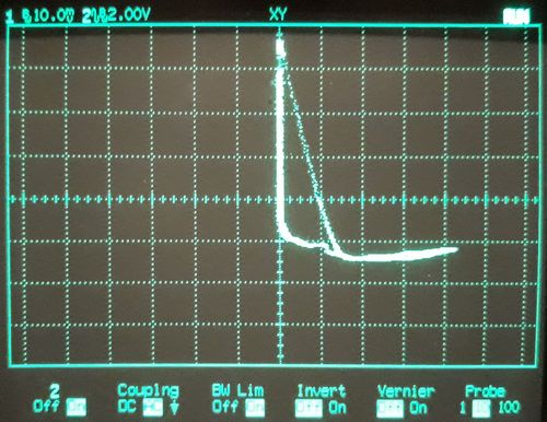
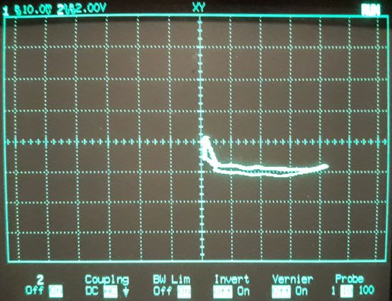
Fig. 18. I-Vd plot of 0C3 voltage regulator: a) Standard connection (Fig. 8); b) "Non-extinguishing" modification (Fig. 17). Horizontal scale -- 10mA/division, vertical scale -- 2V/division.
Fig. 18A shows I-V plot when bleed resistor R2 is removed and V1 tube is allowed to extinguish. It is clear that Vd has to climb by about 11V (vertical section of the trace in the plot) before the discharge re-ignites. Needless to say, the load is subject to the same undesirable overvoltage.
Fig. 18B illustrates Vd behaviour with the bleed resistor of 100K connected (current of about 0.8mA). In this case, a feeble discharge continues glowing in the tube even when load voltage dips below Vr. Usually this "pilot" glow resides on the striker (starter) electrode. It still takes about extra 1.8V (vertical line of the screenshot) for the discharge to slip off the striker pin to the cathode surface. 1.8V overvoltage is negligible compared to 11V in a conventional circuit.
Non-extinguishing circuit (Fig. 17) eliminates a common "failure to ignite" problem. Consequently it helps prevent load overvoltage and allows to increase the ballast resistor R1 and improve efficiency.
Conclusion
With a simple modification as per Fig. 17, glow gas discharge voltage regulator technology is able to compete with and outperform Zener diodes.
Glow discharge circuit (Fig. 17) has the following benchmarks.
- lower and "softer" wide-band noise, easy to suppressed by a small capacitor, no need for a RC filter;
- comparable to Zeners line regulation and better load regulation due to absence of RC filter;
- unconditional tolerance to unlimited filtering capacitor due to the diode load decoupling;
- natural heat dissipation with no need for heatsinks;
- no "failure to ignite" or arc discharge problem due to "pilot glow" technique;
- higher efficiency due to absence of RC filter;
- harmonious fit into vintage radioelectronic devices of the yesteryear;
- nice "cool looking" glow.
Therefore, this novel "incarnation" (Fig. 17) of a glow gas discharge shunt voltage regulator is quite appropriate and highly recommended for retrofitting or upgrading of vintage electronics.

