1. Modulation acceptance and detector loading
Setting an optimum bias to the detector diode, as explained in
Mmax = Zload(Fm) / Rload.
Modulation deeper than Mmax will cause clipping at the troughs of the envelope as the detector capacitor will not be able to discharge deeply and/or fast enough. An example of a bad AM detector design is shown in Fig. 1.

Fig. 1. An example of a bad AM detector design.
In Fig. 1, the detector load R2 is loaded at audio frequencies by the volume control R4=1MOhm and AGC filter R3=1.5MOhm. Effectively connected in parallel, they cause 600kOhm AC loading to the detector. DC load Rload is about 500kOhm (R2+R1), and the overall load Zload at low frequencies is approximately 270kOhm. Thus maximum undistorted modulation is only 54%. At higher modulation frequencies it is be even lower due to combined capacitive loading by C3 and C1. At 8kHz it can handle only up to 31% before diagonal clipping occurs. Such poorly performing circuits like this one are not uncommon in old valve radios.
A better solution is presented in Fig. 2.

Fig. 2. A better AM detector design with the volume control as the DC load.
Here the volume control potentiometer R4 works as the detector load. Input impedance of the audio stage is very high. AGC detector is separate from the audio AM detector. This circuit can accept up to 95% modulation at low frequencies, but obviously at higher frequencies its performance degrades due to C1 and C3 -- to 36% at 8kHz. For both circuits in Fig. 1 and Fig. 2, at full volume position, input capacitance of the first audio stage triode V2, multiplied by the Miller effect to 30...50pF, is added to the total loading capacitance, thus further degrading deep modulation acceptance.
The circuit in Fig. 2 has certain drawbacks. Since DC voltage is present at the volume control potentiometer R4, some crackling may occur during volume adjustment. Because of large time constant R5C5, the audio stage is open to infra-low frequencies. Movements of the volume control, fluctuations of the signal strength on short waves (fading), two stations running at almost the same frequency and creating beats of a few Hertz -- these effects cause swinging of the bias of the first audio stage and possibly the output audio stage, distortion, intermodulation and undulations of the power supply rail of the radio.
Even though the circuit in Fig.2 is preferred, it does not solve the main problem of diagonal clipping at high audio frequencies. Other techniques should be employed to solve this problem.
2. Biased AM detector
An obvious solution is to provide a bias or pull-down, which would overcome the AC loading effect and will enable a detector loading capacitor to discharge fully and fast enough at the envelope troughs. This bias can be provided by connecting the detector load to some fixed voltage source (Fig. 3a), using a voltage divider (Fig. 3b) or a constant current source (Fig. 3c). Unlike in

Fig. 3. AM detectors biased by voltage: a) with pull-down; b) with pull-up and a voltage divider.

Fig. 3c. AM detector biased by a current source bias (or a large resistor).
However, modulation acceptance improvement comes at a price.
Firstly, the bias drastically reduces input impedance of the detector. For example, with 1uA bias, differential resistance of a diode will be about 25kOhm -- far too low to feed the detector directly from a typical high-impedance IF transformer. Therefore, a buffer, for example, a cathode follower shall be used, which adds to the complexity of the circuit.
Secondly, and more importantly, a biased detector, even if it is buffered and even if the diode is ideal, is unable to rectify a small signal below a certain limit. In a conventional (unbiased) detector, ripple at the smoothing capacitor C1 is always in a small proportion to the input level. When the signal is small, the ripple is also small. Thus a conventional detector tends to always track the envelope of the signal. In a biased detector the situation is different. The bias current, discharging C1 with an appreciable slew rate does not allow the ripple to diminish proportionally to the signal. At low signal levels, voltage at C1 tends to follow the input waveform, not its envelope. The diode enters into continuous conduction mode and no longer rectifies the signal. Thus a biased detector is fundamentally unable to accept 100% modulation. It tends to clip the troughs of the envelope. Increasing the bias improves acceptance of high modulation frequencies, but at the same time makes the detector "deaf" to small signals.
To analyze a biased detector it is convenient to introduce a relative bias factor Kb:
Kb = Vbias / Vo,
where Vo -- amplitude of the carrier (maintained by ADC);
Vbias -- DC bias voltage applied to the load (as per Fig. 3a).
A plot below (Fig. 4) illustrates how modulation acceptance of a biased detector depends on the relative bias strength Kb.
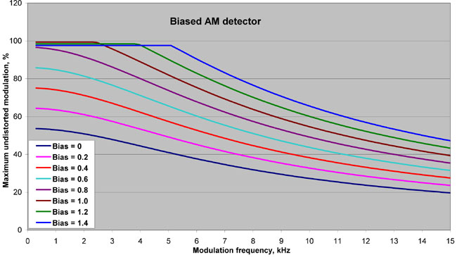
Fig. 4. Undistorted modulation for various bias levels Kb from 0 to 1.4.
In this simulation the detector was loaded by the volume control and by the AGC filter (Fig. 1). The diode is taken to be ideal.
While the bias factor increases from 0 to about 0.9, modulation handling progressively improves. In this range of Kb, the bias helps to overcome loading effects of the volume control and the AGC filter. Further increase of the bias factor Kb (from 1.0 to 1.4) widens the frequency range of distortion-free demodulation, but at the same time reduces acceptance at lower frequencies -- because of the desensitizing effect of the ripple. Therefore, bias shall be applied in moderation. For this particular example, Kb = 1.2 looks a reasonable trade-off. At 8kHz the detector will accept up to 72% modulation, and at the same time desensitization is not too significant, allowing to accept up to 97% at low frequencies.
The following sequence can be used to design a biased detector. A circuit in Fig. 2 is used tn this example -- without extra loading of the detector.
First of all, maximum frequency Fm of full modulation acceptance shall be specified. For medium wave radio stations, Fm = 7kHz may be considered sufficient.
Then, total impedance of the detector load Zload at this frequency Fm shall be calculated. For the circuit in Fig. 2, total impedance Zload(7kHz) = 200kOhm.
Then bias factor is calculated:
Kb = (Rload / Zload) - 1.
For the given example, Kb = 1.5.
Then calculate bias voltage:
Vbias = Kb * Vo,
where Vo is the carrier level at the detector.
For example, if Vo = 4V, bias Vb shall be set at about 6V (Fig. 3a, b).
This concludes the detector optimization as such, but it might be useful to estimate the minimum signal level Mq, relative to Vo, below which the detector ceases to operate linearly and enters a"quadratic" detection mode. It can be shown that:
Mq = 6 * Kb * (Fload / Fif),
where Fif is the carrier frequency;
Fload is the "corner" load frequency, at which |Zload| drops by -3dB relative to its low frequency value.
In our example (Fig. 3b), Fif = 455kHz and Fload = 3kHz. gives Mq = 6%. These 6% is the "sacrifice" for extending its frequency range to 7kHz. The biased detector will not be able to accept more than 94% modulation.
When the signal level drops below Mq*Vo (240mV in our example), the detector still rectifies the signal, but in a nonlinear (quadratic) mode. When the signal drops further below 1 * Kb * (Fload / Fif), or 40mV in our example, the diode will cease to rectify completely. Note that a conventional unbiased diode detector would have continued to operate down to 25mV and even lower as explained in another article.
A constant current biased detector (Fig. 3c) optimization technique is slightly different.
Firstly, its load capacitor C1 is selected large enough, so that its impedance at the maximum modulation frequency Fm is significantly lower than all the other loads combined. For example, for a typical 500kOhm volume control, C1 can be chosen 220pF (about 100kOhm impedance at 8kHz).
Then, knowing typical expected signal level Vo at the detector, bias current Ib can be calculated:
Ib[uA] = 6.3 * Vo[V] * Fm[kHz] * C1[nF].
In our example, for Vo = 4V, Fm = 8kHz, C1 = 0.22nF, optimum bias current should be about Ib = 40uA. Setting such current would require a 6.2MOhm resistor from +250V rail to the detector diode, as per Fig. 3c.
Amount of "sacrificed" modulation, lost to the ripple, can be estimated by:
Mq = 6 * (Fm / Fif),
which amounts to 10% in the example.
As demonstrated, constant current biasing method gives slightly worse performance results, but less sensitive to the additional loading by the volume control potentiometer.
Optimum performance (modulation acceptance) for both variants of the biased detector can be achieved only at a certain signal level Vo. Higher Vo is equivalent to lower Kb, and the detector behavior approaches that of a conventional unbiased detector. In a current biased detector (Fig. 3c) modulation bandwidth is inversely proportional to the signal level. If the input level Vo decreases, while the sensitivity floor, determined by the ripple, remains the same, modulation acceptance falls sharply. Therefore, to use a biased detector effectively, a receiver shall have plenty of gain and a very effective AGC maintaining signal at the detector close to the optimum Vo level.
A practical biased detector circuit is shown in Fig. 5.
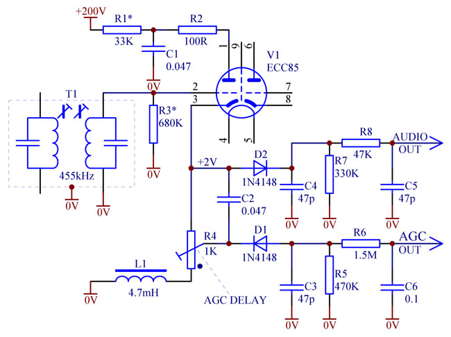
Fig. 5. Biased AM detector with delayed AGC.
Self-bias voltage for the triode V1 is used as a bias voltage for the AM detector D2. The same self-bias voltage or a part thereof adjusted by R4 is used to reverse bias an AGC detector D1 to set a certain AGC threshold -- "AGC delay".
The cathode follower has a very high input resistance. Sometimes, if the cathode circuit has excessive capacitance to ground, together with cathode-grid capacitance of the valve, the circuit tends to work similarly as a Colpits oscillator, introducing negative resistance into the input LC tank. It creates regeneration, Q-multiplication and in some cases oscillations in the cathode follower. Excessive Q factor on the IF transformer secondary is not desirable, as it may distort the passband response of the IF chain, so R3 may be used to bring its Q factor to the same value as on the primary.
3. Emitter detector
An emitter detector (Fig. 6) is perhaps the best and the most effective way to utilize a biased detector principle.

Fig. 6. Emitter detector with an active AGC.
One transistor Q1 works as a buffer (emitter follower) and as a detector at the same time. You might notice that the loading capacitor C1 is connected to the collector, not to ground as commonly done. This is to reduce IF harmonics emission. Current through Q1 and C1 flows in short pulses. If C1 is mounted on short leads close to Q1, then these current pulses circulate only through this small loop and electromagnetic radiation is minimal. If C1 were connected to ground, the current pulses would have to find their way through the wiring and decoupling capacitor C2. Surely it would be a longer path and larger radiation loop.
A typical general purpose transistor has relatively small reverse emitter-base breakdown voltage. Most transistors are rated at 5V, but in reality can withstand up to 7V. Some more "exotic" transistors, like STX13003 or STX83003, are rated at 9...18V, but these parts are not recommended due to lower current gain (beta), larger junction capacitance and narrower bandwidth. Therefore, given that the reverse emitter junction voltage shall not exceed 5...7V, the detector can handle the carrier amplitude up to a quarter of that value, i.e. up to about 1.5V. To allow for some headroom it is recommended to have Vo = 1...1.2V.
With such stringent limitations on Vo, a radio has to have a perfect automatic gain control (AGC), accurately maintaining the input signal to the detector. Only an active, amplified AGC can satisfy such requirements. In this example, an active integrator based AGC consists of a composite gain stage Q2Q3 and integrating circuit R3C5. Gain of this stage is above 1000. Capacitors C3 and C4 are there merely for noise filtering. Resistor R9 sets the initial AGC voltage. For some old radios with 6A8, 6K8, 6J8, 6SA7, 6K7, 6SK7 tubes operating without self-bias, initial AGC level shall be set at -3V. For newer and European radios where each tube is self-biased, AGC can start from 0V and R9 can be removed.
Base-emitter voltage of Q2 serves as a reference voltage to set the AGC threshold or "AGC delay". With Vbe = 0.6V, R6 = 1.5MOhm and R3 = 1 MOhm, the AGC will start operating once average DC voltage on the emitter of Q1 exceeds approximately 0.4V. Given Vbe = 0.6V for Q1, the AGC integrator will start working once the IF amplitude Vo at the Q1 base reaches 0.4V + 0.6V = 1V. The integrator will tend to precisely maintain this level of Vo. AGC delay threshold can be changed by adjusting R6.
Very stable Vo in this circuit helps run the biased detector Q1 in the optimum mode. The bias is set by R4. With Q1 removed, the bias voltage on R1 would be about --1V. However, with no signal and the transistor fitted, the emitter voltage is --0.6V, so the effective detector bias Vbias is 0.4V. That is why Kb = 0.4 in this circuit.
With a mild bias factor of Kb = 0.4, the detector accepts nearly 100% modulation up to 8kHz. The circuit can be assembled on a small piece of a prototype board and fitted into almost any tube radio. Sound quality will markedly improve and the radio will be more convenient to use as the AGC perfectly levels out volume of all the stations, and there is no need to tweak volume control while moving the dial.
Bias detectors described above offer a better modulation acceptance over the audio frequency range, but have certain drawbacks. They work well only at a certain signal level and therefore require a very good amplified AGC. A question remains whether it is still possible to improve a conventional unbiased detector to widen its bandwidth without sacrificing sensitivity to the ripple. Fortunately, the answer to this question is "Yes".
4. Inductive compensation
In a conventional diode detector, it is the capacitor which limits the slew rate and causes the diagonal clipping distortion. How would you neutralize a troublesome capacitance? Obviously, by a compensating inductor. This method is described below (Fig. 7).
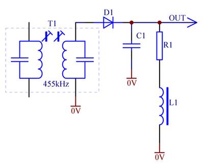
Fig. 7. Inductive compensation of a detector load.
Inductor L1 together with the capacitor C1 form a low-Q LC tank tuned to high audio frequencies. Because of the resonance, total load impedance somewhat increases above the value of R1 (Rload) in a certain frequency range, as opposed to decreasing in a conventional detector. For typical R1 values of hundreds of kiloOhms, the inductor value would be of the order of 10H, which is too large to consider a real wirewound choke. An emulated inductor can be implemented instead, as shown in Fig. 8.
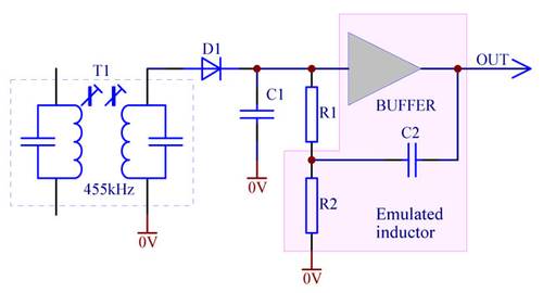
Fig. 8. Load compensation by an emulated inductor.
At high frequencies the bottom end of R1 has almost the same potential as the top end, and the current through R1 remains almost constant -- the same effect as a real inductor would have had. The circuit simulation results will be discussed later, but here it can be pointed out that the widest modulation acceptance bandwidth can be achieved if R1*C1 = L1 / R1 (Fig. 7) or if R1*C1 = R2*C2 (Fig. 8), on condition that R2 << R1 and the buffer gain is unity. Further, it turns out that the detector can accept 100% modulation up to about 1.4*Fload. It is a remarkable result. While in a conventional detector modulation acceptance drops to 71% at Fload, in the inductively compensated detector 100% acceptance extends to 1.4*Fload.
The following design sequence is recommended.
Firstly, a maximum frequency of 100% modulation acceptance Fm shall be set. Suppose Fm = 9kHz, which is more than enough for an AM radio.
Then Fload can be calculated: Fload = 0.7*Fm. For this example, Fload = 6.3kHz.
After that, knowing R1, select C1 to get the target Fload:
C1[pF] = 1000000 / (6.3 * Fload[kHz] * R1[kOhm]).
In this example, for Fload = 6.3kHz and R1 = 470kOhm, C1 = 51pF.
Lastly, select R2 much smaller than R1, say twenty times smaller, and calculate C2 = R1 * C1 / R2. For example, if R2 = 22kOhm, C2 = 1000pF.
Performance of such inductively compensated unbiased detector does not depend on the signal strength -- it can be as low as the diode can handle (down to 25mV) and as high as the buffer can handle.
5. Positive feedback enhanced detector ("magic capacitor")
Another method of improving modulation acceptance to 100% over a wide range of frequencies is presented below. How wonderful it would be to get hold of some "magic capacitor" which would have zero capacitance at audio frequencies (to avoid diagonal clipping) and at the same time a large capacitance at IF to keep the ripple to a minimum (Fig. 9). That would have solved all the problems.
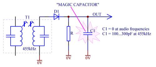
Fig. 9. A hypothetical "magic capacitor" based AM detector.
Surprisingly, such "magic capacitor" can be easily created. To do so, the load capacitor C1 in the detector shall be connected to the output of a low-pass filter (Fig. 10).
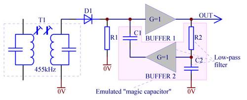
Fig. 10. Emulation of the "magic capacitor" by positive feedback.
Cut-off frequency of the low-pass filter is set above the audio range, but below IF. At audio frequencies, when the gain of the filter is close to unity, both plates (ends) of C1 are almost equipotential, and practically no AC current is flowing through C1. Thus C1 is virtually out of circuit at audio frequencies. At high intermediate frequency, when the filter gain is close to zero, the bottom end of the capacitor appears practically grounded, thus the capacitor is fully in circuit and serves its main purpose to smooth the rectification ripple. The circuit can be further simplified as shown in Fig. 11.
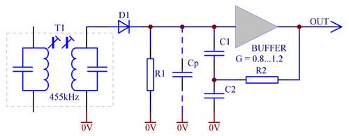
Fig. 11. Simplified "magic capacitor" feedback configuration.
If C2 >> C1, then C1 becomes the "magic capacitor", and R2C2 form the low-pass filter. "Magic capacitor" method is more flexible and "aggressive" than inductive compensation method in terms of broadening the modulation acceptance frequency range. Besides, unlike the inductive compensation method, it does not require Fload to be of a certain value. A larger than usual C1 can be chosen to minimize ripple, because C1 ("magically") will cause no loading at all at audio frequencies. Simulation proves that the "magic" also takes out the shunting capacitance Cp (diode and wiring).
To some readers the capacitive divider C1C2, the buffer and R2 might strikingly resemble a part of a Colpits oscillator -- without a coil though. Such observation indeed has an important bearing. Similar to a Colpits oscillator, this configuration does introduce negative resistance into the circuit, partly canceling loading effect of R1. Ramifications of this phenomenon will be discussed later.
Comparative results of simulation of the inductively compensated detector and the "magic capacitor" detector are presented in a plot (Fig. 12) below.
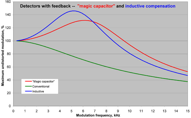
Fig. 12. Modulation acceptance for detectors with inductive compensation and "magic capacitor".
The plots of modulation acceptance were simulated for the following conditions:
a) "Magic capacitor": R1 = 470K; C1 = 56pF; Cp = 5pF; C2 = 560pF; R2 = 27K (Filter cut-off 10kHz); Buffer gain = 0.9.
b) Conventional AM detector: R1 = 470K; C1 = 56pF; Cp = 5pF, no other loads on the detector.
c) Inductive compensation: R1 = 470K; C1 = 51pF; Cp = 5pF; C2 = 5600pF; R2 = 4.7K (R2C2 corner 6.3kHz); Buffer gain = 1.0.
It might surprise a reader that undistorted modulation values on the vertical axis exceed 100%. An an envelope detector, indeed, can not demodulate overmodulated signal without distortion. In this graph, vertical axis in fact shows Zload / Rload ratio. Values above 100% simply indicate that at certain modulation frequencies the detector loading is even less than for DC. In other words, 100% modulation can be easily accepted without clipping at these frequencies. However, this statement is true if the detector is fed from a zero-impedance IF source. If the detector is connected directly to a high-impedance IF transformer, modulation "enhancement" or even overmodulation can take place.
6. Modulation suppression, enhancement, overmodulation and detector load equalization
It is a common knowledge that capacitive loading of a diode detector results in diagonal clipping. A less known fact is that the same capacitive loading can also reduce modulation index at a high-impedance source, if the detector is directly connected to the source, e.g., IF transformer. The explanation is as follows.
In a steady state, all the power drawn by the detector from the source is dissipated in the load resistor Rload. and the detector loads the source with an equivalent load Rload / 2. If the detector is capacitively loaded, and while the signal is rising, more power than in a steady state is drawn from the source to charge the loading capacitor in addition to Rload dissipation. Thus the rising slope of the envelope gets somehow suppressed, squashes. When the signal is falling, some stored energy from the capacitor feeds the load resistor, so less power than in steady state is drawn from the source, the source is getting underloaded, and the troughs of the envelope become shallower. Overall, this is equivalent to modulation reduction (suppression) at the source.
A similar but reverse phenomenon takes place if the load impedance Zload at some frequencies exceeds Rload. When the signal is rising, the positive feedback (negative impedance) in the magic capacitor detector circuit or a resonance in the inductively compensated detector tends to "help" the detector voltage rising, thus less power is being drawn from the source and the envelope peaks are emphasized (enhanced). When the envelope is going down, the same feedback "helps" to pull the detector voltage down, to ground, excessively damping the source trough the diode. Thus the envelope troughs get deeper. Overall, it is equivalent to increasing or enhancing modulation at the source.
The above modulation suppression or enhancement effects are more pronounced when the source impedance is large compared to the average detector input impedance (about Rload / 2). If the source is low impedance, the above effects manifest to a little extent, or not at all if a detector is fed from a low output impedance buffer.
Such enhancement works somewhat like a treble boost tone control and may be even desirable to some extent. Sound becomes crispy, light, "airy", transparent. But if initial modulation is already close to 100% (for example, during fading), then its further enhancement can result in overmodulation and distortion. Boosting of the peaks is not a problem, but it is the troughs that will "hit the ground" and be clipped. That is why an "aggressive" compensation (as shown in Fig. 12) where the AC load Zload can significantly exceed the DC load Rload is not desirable if the detector is directly connected to an IF transformer.
Therefore, by selecting the circuit parameters accordingly, it is better to keep Zoad "flatter" over the audio frequency range as illustrated in Fig.13.
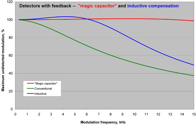
Fig. 13. Load equalisation for for detectors with inductive compensation and "magic capacitor".
The plots of modulation acceptance were simulated for the following conditions:
a) "Magic capacitor": R1 = 470K; C1 = 56pF; Cp = 5pF; C2 = 560pF; R2 = 2.7K (R2C2 cut-off 100kHz); Buffer gain = 0.82.
b) Conventional AM detector: R1 = 470K; C1 = 56pF; Cp = 5pF, no other loads on the detector.
c) Inductive compensation: R1 = 470K; C1 = 51pF; Cp = 5pF; C2 = 5600pF; R2 = 2.4K (R2C2 cut-off 12kHz); Buffer gain = 1.0.
To achieve a flat loading in a inductively compensated detector, R2C2 = 0.5 * R1C1. Acceptance of 100% modulation extends only to Fload (where a conventional detector reaches only 71%). It is a considerable improvement.
"Magic capacitor" method can be far more effective. Setting the low-pass filter cut-off frequency up to 100kHz greatly extends the 100% modulation acceptance range -- even broader than necessary (Fig. 13, red curve). By reducing the buffer gain, Zload peaking can be eliminated. It is a convenient feature as a simple cathode follower used as the buffer would naturally have gain below unity. Gain can be further reduced by shunting C2 with a resistor. An alternative method of peaking reduction is to deliberately increase parallel capacitance Cp.
"Magic capacitor" feedback method is much more versatile, effective, flexible, and therefore preferred to the inductive compensation. Analytical calculations with so many variables are impractical. It is recommended to use simulation in SPICE or by this crude downloadable spreadsheet.
7. Practical "magic capacitor" feedback detector circuits

Fig. 14. An envelope AM detector and AGC in the synchronous detector module SD-7.
A quality AM detector section (Fig. 14) in SD-7 synchronous detector module uses the "magic capacitor" feedback configuration, IC2A acting as a buffer. The detector diode D2 is biased by a forward voltage across D1 and also through R4. Bias factor Kb is mild -- about 0.5. The detector is fed from a low impedance preamplifier IC1A, therefore detector load impedance peaking does not cause overmodulation. R5 decouples capacitive load C4C5 from the operational amplifier. AGC integrator is similar to the one described in section 3 (Fig. 6), but a regulated -5V reference voltage and R11 are used to set the AGC threshold ("AGC delay"). In this case, high performance AGC is needed not for the AM detector, but to keep optimum PLL loop gain in the synchronous detector section. D3 prevents from the integrator input voltage going negative under no signal condition, thus slightly improving the AGC reaction time.
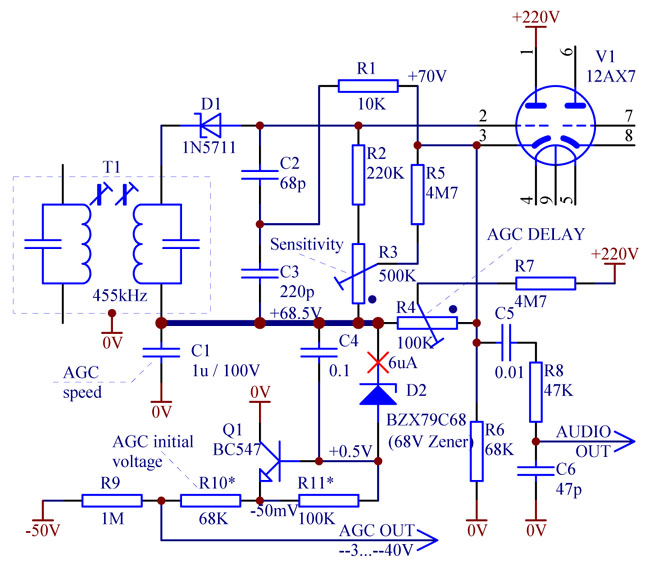
Fig. 15. "Magic capacitor" AM detector with efficient amplified delayed AGC.
A circuit in Fig. 15 combines a "magic capacitor" feedback detector and an AGC amplifier. The detector virtual floating "ground" rail is shown as a bold trace. Without a signal, since V1 cathode voltage is 1.5...2V higher than grid voltage, a current of 15...20uA flows through R4 and develops +68V across the Zener diode D2. (Ignore R7 for now, its purpose will be explained later.) Transistor Q1 is held in saturation, adding 0.5V to the Zener. Thus the virtual detector rail is held at about +68.5V.
The detector itself uses a low-capacitance Schottky diode D1, a relatively high load R2+R3 to minimize IF transformer shunting and employs the "magic capacitor" feedback through R1 to the junction of C3 and C2. Low-pass filter cutoff is about 70kHz which would give a rather flat equalized loading impedance, as demonstrated above. Triode V1 is works as a buffer with a gain of about 0.97. Note that R5 and R3 allow to forward bias the diode slightly -- just to bring the diode to the edge of conduction and maximize sensitivity for small signals, as explained in the other article. With such a small bias the detector in Fig. 15 is not qualified as a biased detector in the context of this article. Trimmer R3 can be used to adjust the bias for maximum sensitivity to the smallest signals -- for example, static IF stage noise.
Automatic gain control (AGC) works as follows. With the input IF signal increasing, the detector D1 is developing more negative voltage on the grid, and consequently the cathode voltage is going down. Current through R4 is diminishing. Eventually, at some point, when the current drops to about 6uA (set by Vbe = 0.6V / R11), it will no longer will be sufficient to keep Q1 in saturation. Q1 base voltage and the virtual detector "ground" rail would go down, with Zener D2 still in regulation. This point is the threshold of AGC operation (AGC delay). Transistor Q1 now operates as an emitter follower, sending the AGC control voltage to the remote cut-off tubes of the receiver.
Slow variations of the detector voltage are fed back (reflex, recirculated) from the cathode back to the detector floating "ground" rail through R4C1 filter. Thus, slow changes of the detector voltage get applied virtually between grid and cathode. The valve operates as an AGC mu-amplifier with a floating source, cathode load and gain of about 50. At the same time, at audio frequencies, the valve works as a cathode follower (with gain of about 0.97) since the detector virtual "ground" is virtually grounded via C1 at audio frequencies.
AGC threshold is determined by the difference between the initial current through D2 and the current at the point of Q1 exiting saturation mode. To reduce the threshold, the later current can be increased by lowering R11. To raise the AGC threshold, cathode voltage shall be raised by either increasing the plate voltage or using a triode with a lower amplification factor, e.g., ECC85 (6AQ8), 12AT7. Alternatively, one can inject additional current into the virtual "ground" rail of the detector. Resistor R7 is provided for that, and trimmer R4 can be used to adjust this injected current. It is recommended to set AGC threshold to 1...2V.
The circuit in Fig. 15 has been successfully tested in a Philips 5-valve vintage radio and gave excellent results. If a radio uses octal valves, 6SL7 is recommended as V1. The second triode can be employed as the first audio amplifier stage.
Triode V1 is utilized quite efficiently in this circuit -- the single tube works as a feedback buffer for the "magic capacitor", as an audio buffer, as an AGC amplifier, provides floating bias for the detector diode and provides reference voltage for the AGC delay. Not bad for an old tired triode, isn't it?
